Advanced Techniques and Industry Standards in LED Display Manufacturing
The LED display industry has seen remarkable advancements over the past decade, driven by technological innovation, increasing demand for high-resolution and energy-efficient screens, and the integration of smart functionalities. As a professional engineer specializing in LED LCD screen manufacturing, this article provides an authoritative overview of key manufacturing techniques, quality standards, and technical parameters essential for producing superior LED displays that meet global commercial and consumer demands.
Introduction
LED displays form the backbone of digital signage, broadcast, and consumer electronics, offering vibrant colors, high brightness, and versatile form factors. The manufacturing process for LED displays is complex, involving semiconductor fabrication, PCB assembly, optical calibration, and rigorous quality assurance to ensure optimal visual performance and durability. This article delves into the critical aspects of LED display manufacturing including material selection, chip technology, mounting methods, and testing standards, highlighting the latest industry practices based on experience and authoritative sources such as the IEC 62087 and ANSI/IES TM-30-20 standards.
Material Selection and Semiconductor Technology
The foundation of any LED display is its light-emitting diode’s semiconductor chip. The most prevalent material system is Gallium Nitride (GaN) for blue and green LEDs and Gallium Arsenide (GaAs) or Aluminum Gallium Indium Phosphide (AlGaInP) for red LEDs. GaN-based LEDs have revolutionized the industry by enabling high-brightness blue and green components, which combined with phosphor coatings produce a broad color gamut essential for Ultra High Definition (UHD) displays offered by brands like Samsung and LG. Precise control over epitaxial layer thickness and doping during Metal-Organic Chemical Vapor Deposition (MOCVD) growth processes determines chip efficiency, wavelength stability, and lifespan.
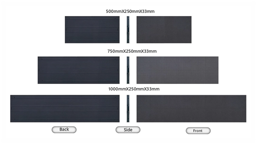
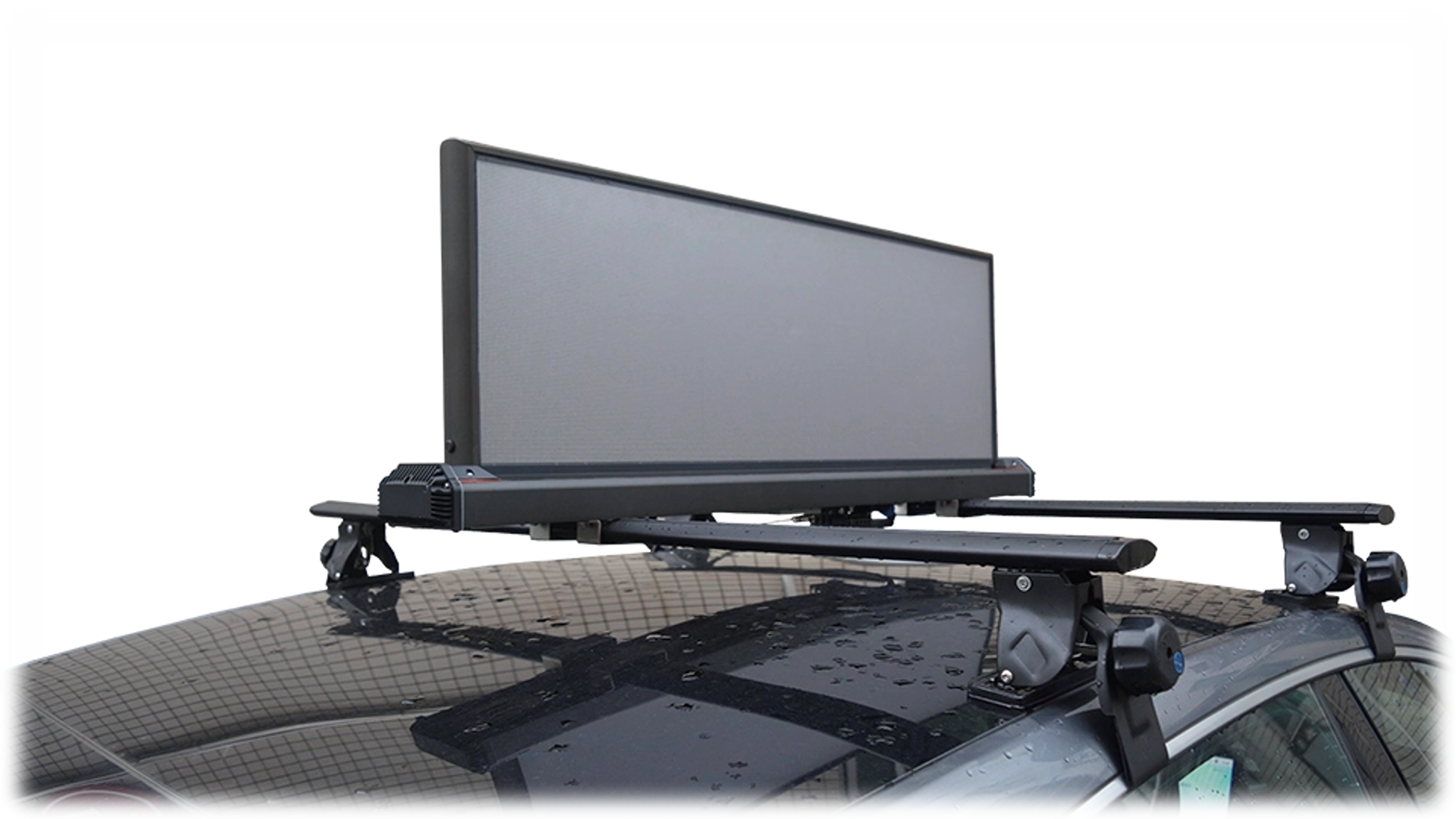
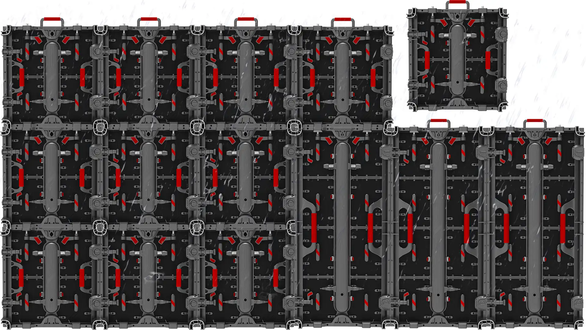
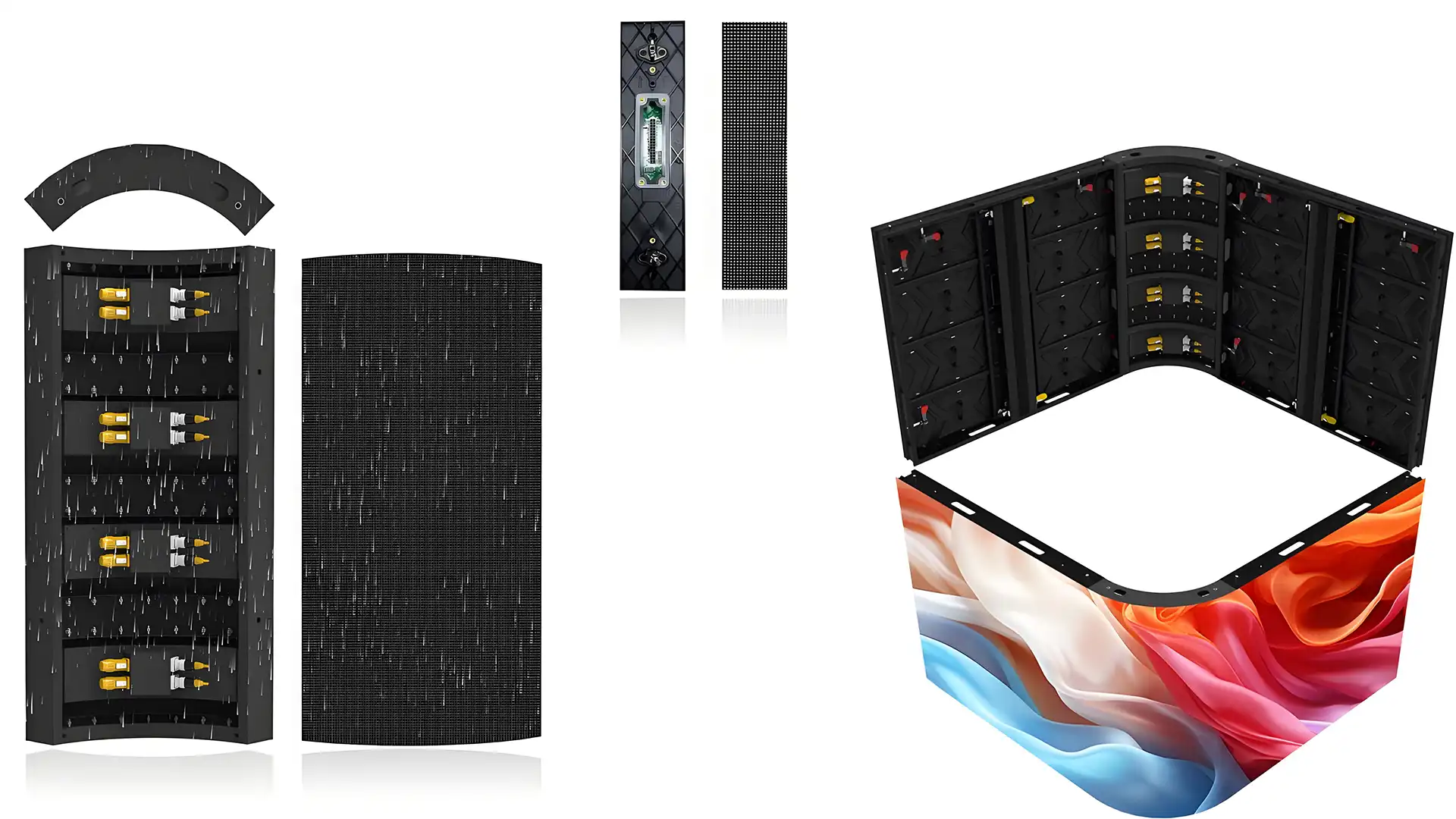
Mounting Techniques: SMD vs. COB
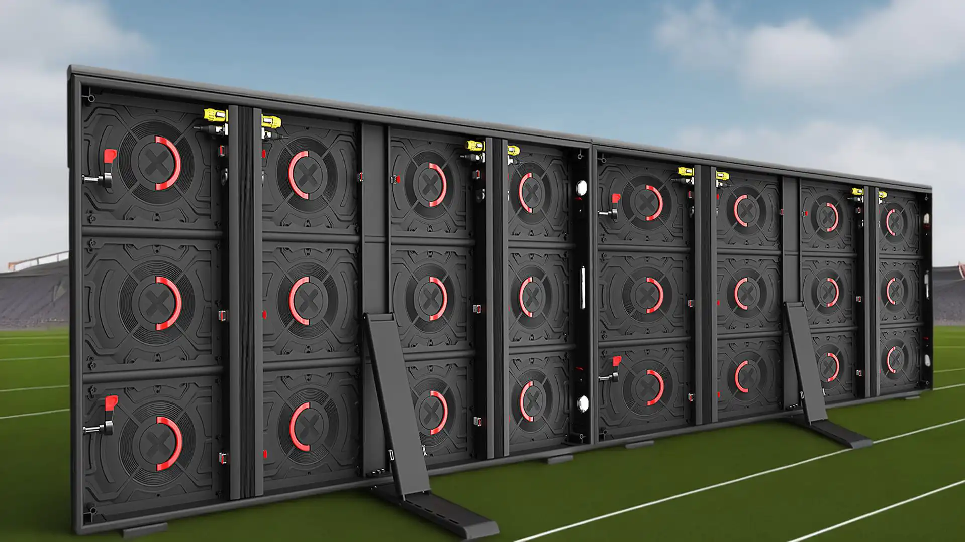
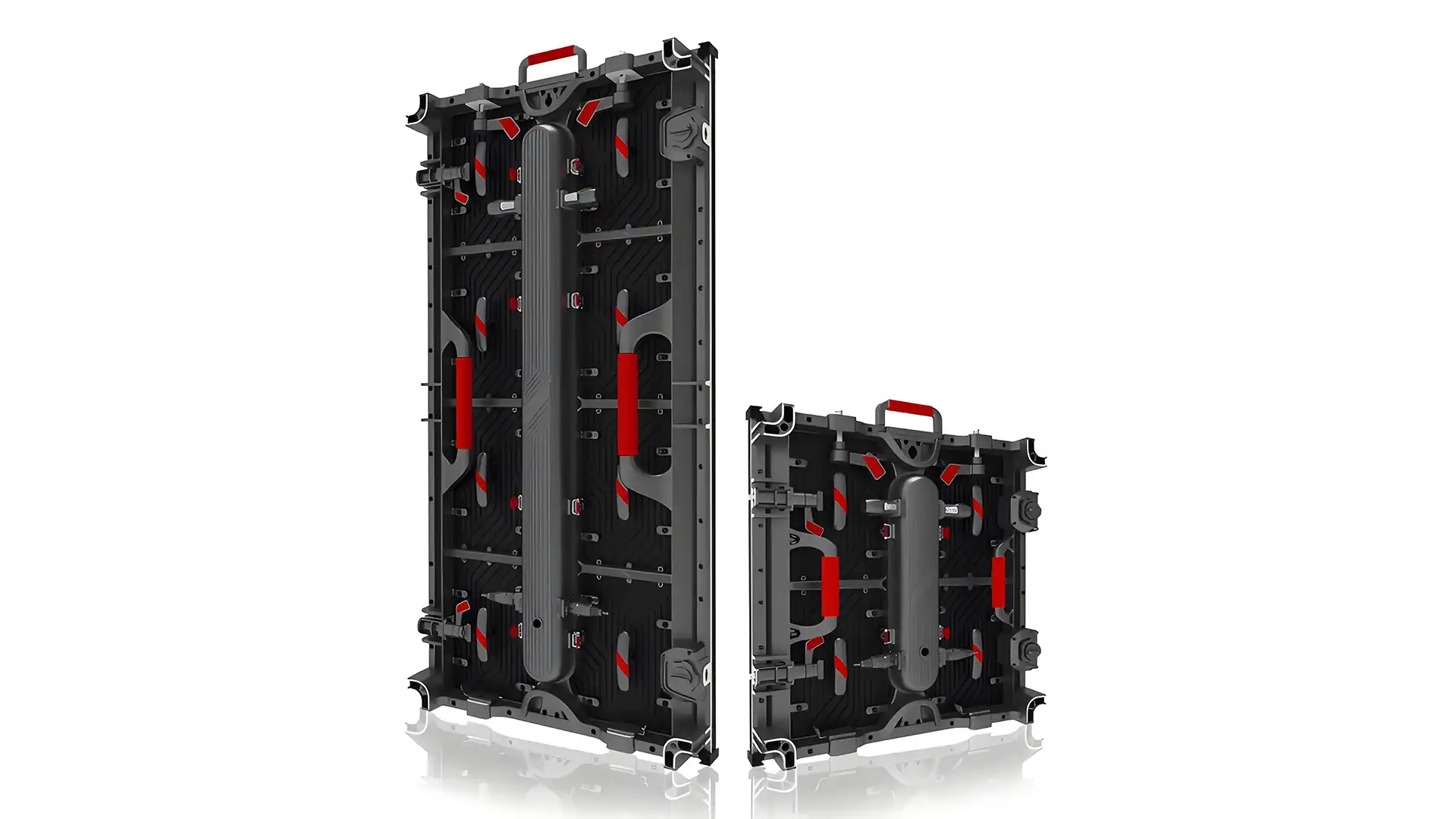
Two dominant LED mounting techniques are Surface-Mount Device (SMD) and Chip-on-Board (COB). SMD LEDs are mounted on a PCB substrate with individual lenses for each primary color, offering pixel pitches down to 0.5mm. This makes SMD suitable for fine-pitch indoor displays requiring high pixel density. In contrast, COB technology involves directly mounting LED chips on a substrate creating a single module that simplifies assembly and improves heat dissipation. COB is often preferred for outdoor signage due to its robustness and superior thermal management, which enhances lifespan under variable environmental conditions.
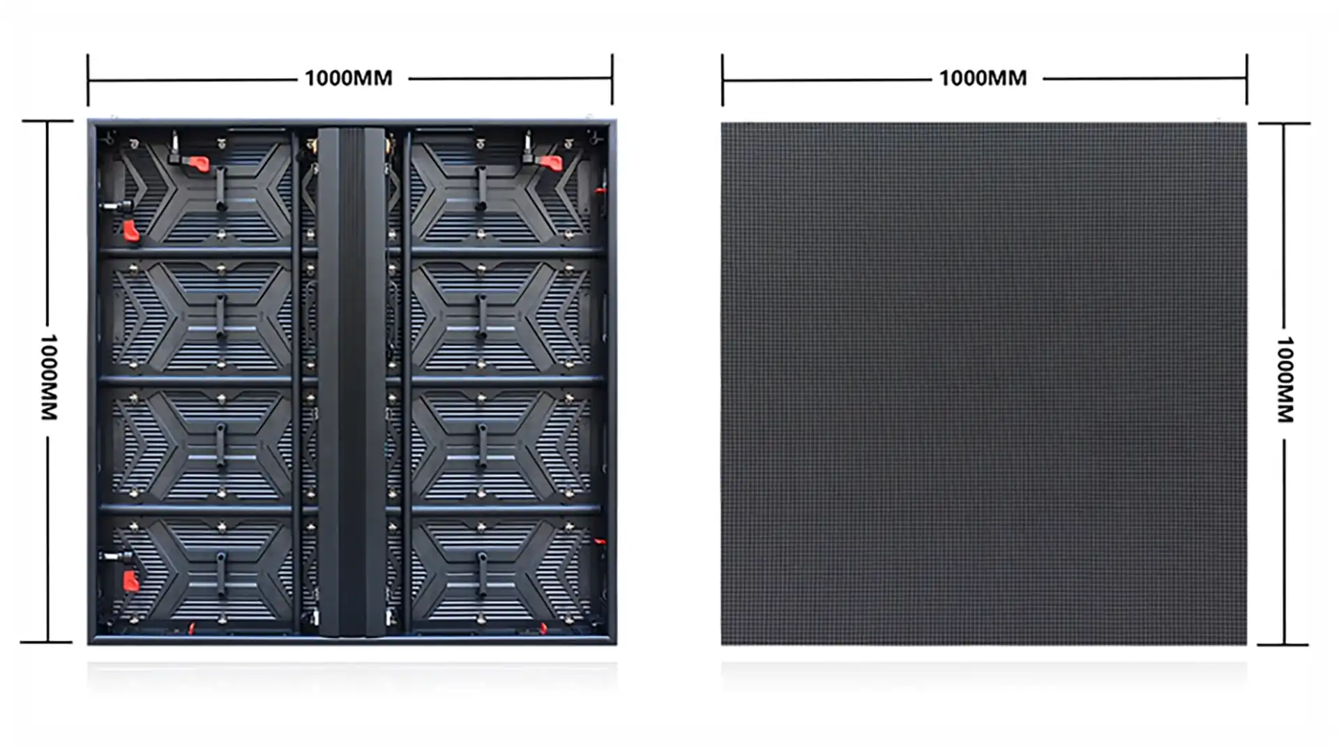
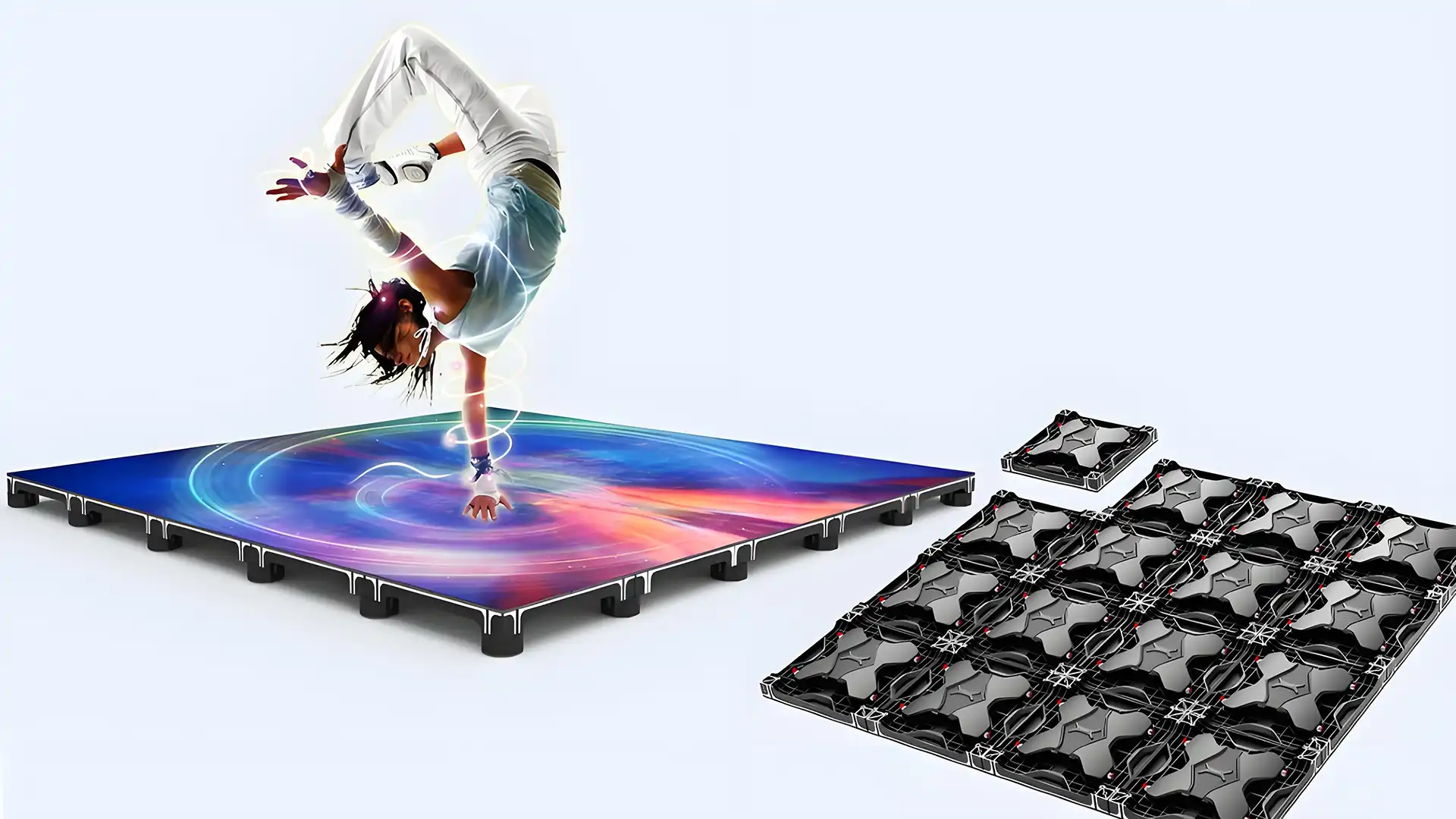
Pixel Pitch and Resolution Standards
Pixel pitch, the distance from the center of one LED cluster (pixel) to the next, directly affects resolution and viewing distance. Standard indoor displays range between 0.5mm and 4mm pixel pitch, while outdoor displays typically exceed 4mm due to cost and viewing distance requirements. According to the International Electrotechnical Commission (IEC) 62087 standards, manufacturers should align pixel pitch and brightness levels (minimum 1000 cd/m² for indoor and above 5000 cd/m² for outdoor) to optimize legibility and visual comfort. Achieving true 4K resolution at a practical size requires ultra-fine pixel pitches and consistent color calibration ensuring accurate chromaticity coordinates (x,y) within ±0.01 on the CIE 1931 color space.
Quality Assurance and Reliability Testing
Reliability in LED display manufacturing hinges on comprehensive testing regimes. Key tests prescribed by ANSI/IES TM-30-20 include color rendering index (CRI) and gamut area index (GAI) measurements to validate color fidelity. Thermal cycling tests ensure LED chips and drivers withstand temperature ranges typically from -40°C to +85°C for outdoor-rated products. Moisture ingress and IP rating verification—commonly IP65 or higher for outdoor units—are critical to prevent premature failure. Electrical testing for forward voltage (typically 2.8V for red LEDs and 3.2V for blue/green LEDs) and luminous flux measurements guarantee consistency from batch to batch.
Energy Efficiency and Environmental Impact
Energy efficiency is a paramount consideration in today’s LED manufacturing ecosystem. Modern LEDs achieve luminous efficacies exceeding 150 lm/W, significantly reducing power consumption compared to legacy display technologies like plasma or LCD backlit. Compliance with environmental standards such as RoHS (Restriction of Hazardous Substances) and WEEE (Waste Electrical and Electronic Equipment) ensures that no hazardous materials compromise environmental safety. Manufacturers increasingly adopt recycling protocols and extended producer responsibility (EPR) frameworks to sustain long-term ecological balance.
Conclusion
Manufacturing advanced LED displays requires a multidisciplinary approach encompassing semiconductor physics, mechanical engineering, optics, and stringent quality control aligned with global standards. By emphasizing precision in chip fabrication, selecting optimal mounting technologies, adhering to recognized pixel pitch and brightness standards, and performing extensive reliability testing, manufacturers deliver products that fulfill the rising expectations of clarity, durability, and efficiency. As the industry advances toward microLED and flexible displays, the foundational manufacturing principles outlined here remain essential to innovation and market success.
References:
- IEC 62087 Ed. 3.0: Methods of measurement for the power consumption of audio, video and related equipment.
- ANSI/IES TM-30-20: IES Method for Evaluating Light Source Color Rendition.
- “Semiconductor LED Manufacturing Techniques,” IEEE Journal on Selected Topics in Quantum Electronics, 2021.
- Samsung Display Technical White Paper, 2023.
- LG Electronics Environmental Compliance Reports, 2022.