Advanced Technologies and Manufacturing Processes in LED Display Production
The LED display industry has witnessed significant advancements over the past decade, driven by evolving consumer demands, improved materials science, and innovative manufacturing techniques. As a professional LED display engineer, I have observed that the convergence of cutting-edge technologies and optimized production processes has fundamentally transformed LED display manufacturing, resulting in higher performance, better reliability, and enhanced visual quality.
Overview of LED Display Technologies
LED (Light Emitting Diode) displays rely on semiconductor diodes that emit light when electrically energized. They are characterized by their superior brightness, energy efficiency, and long life span compared to traditional display technologies like LCD or CRT.
There are several key types of LED displays used globally:
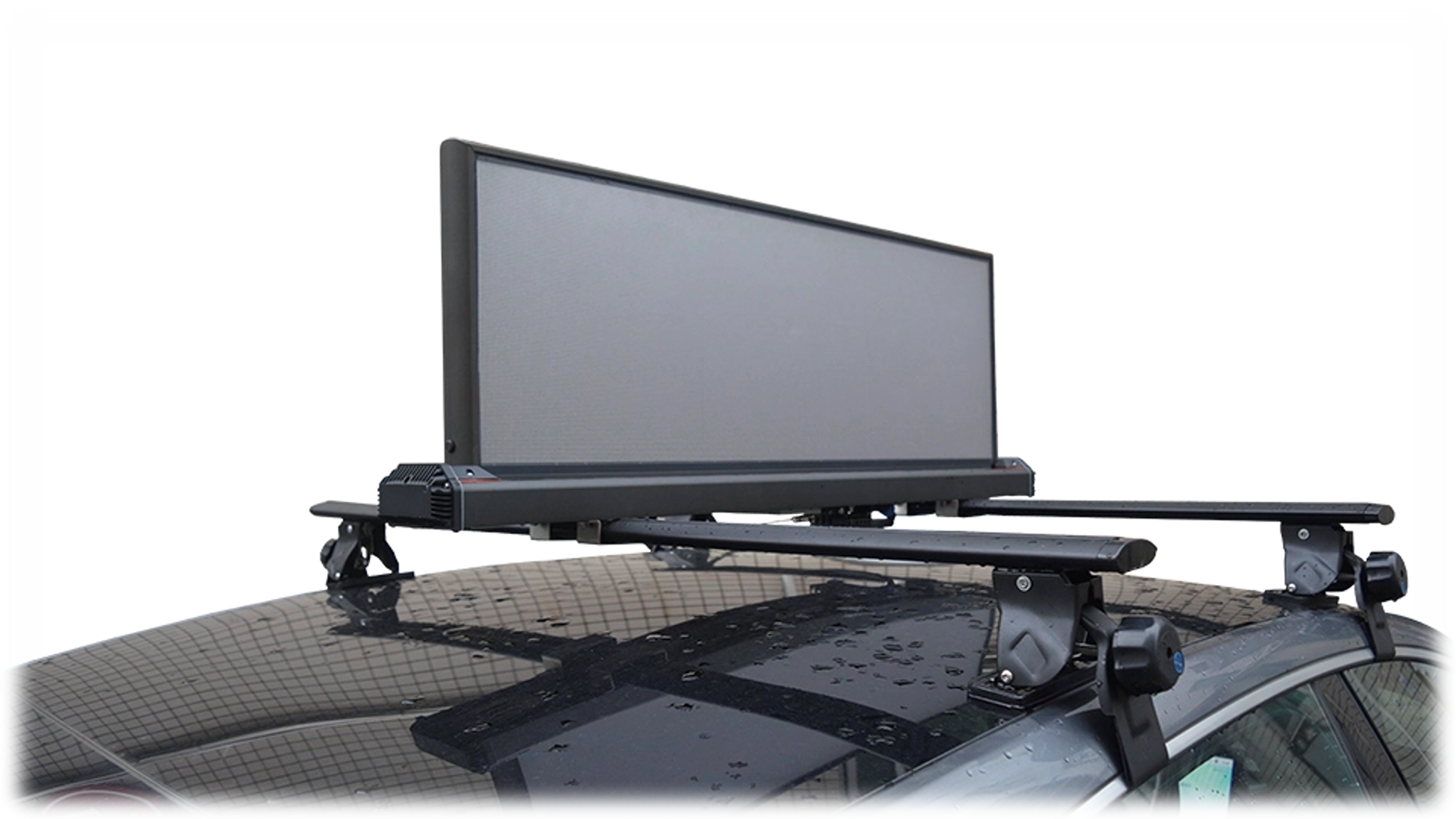
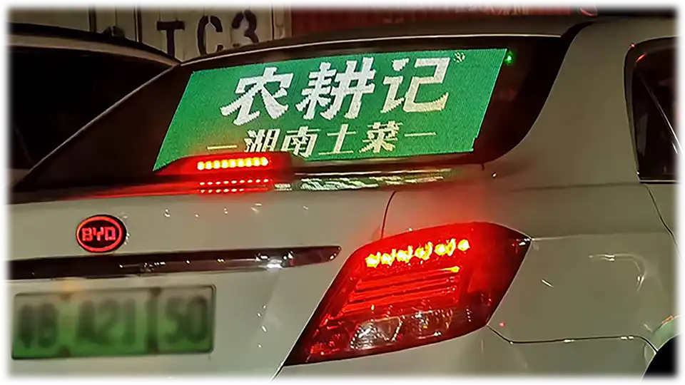
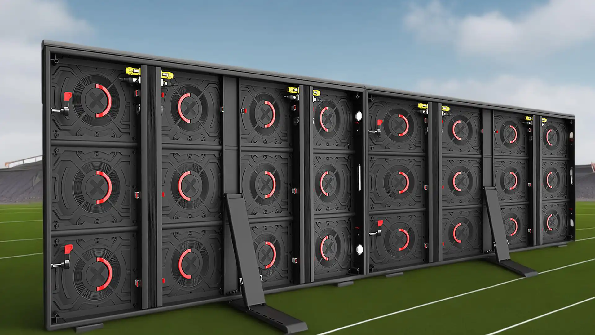
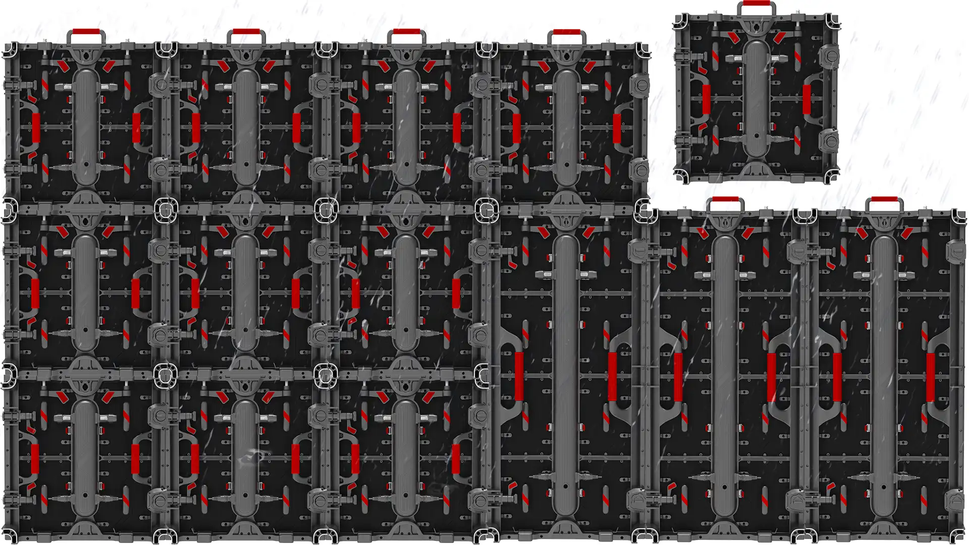
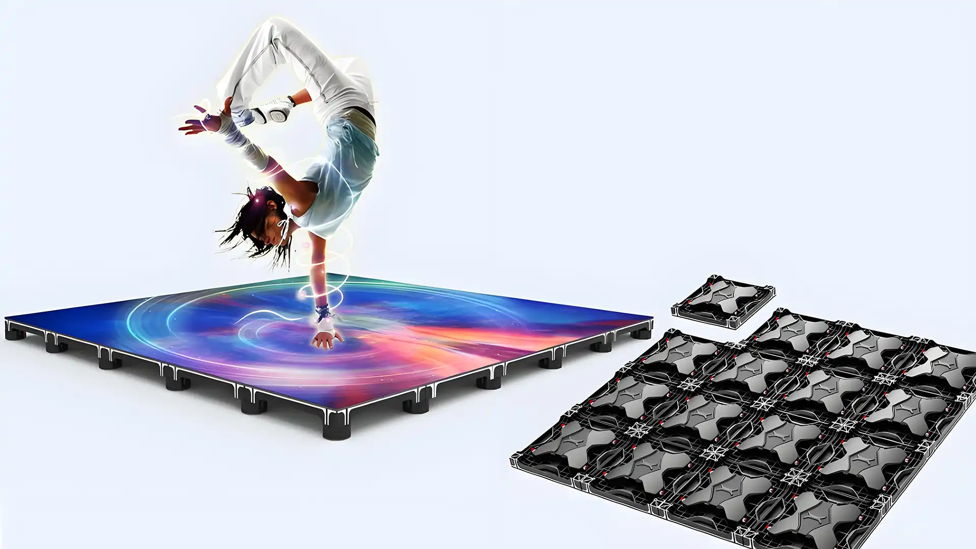
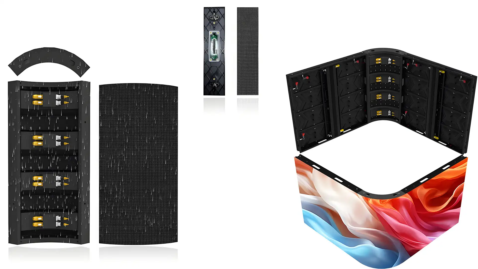
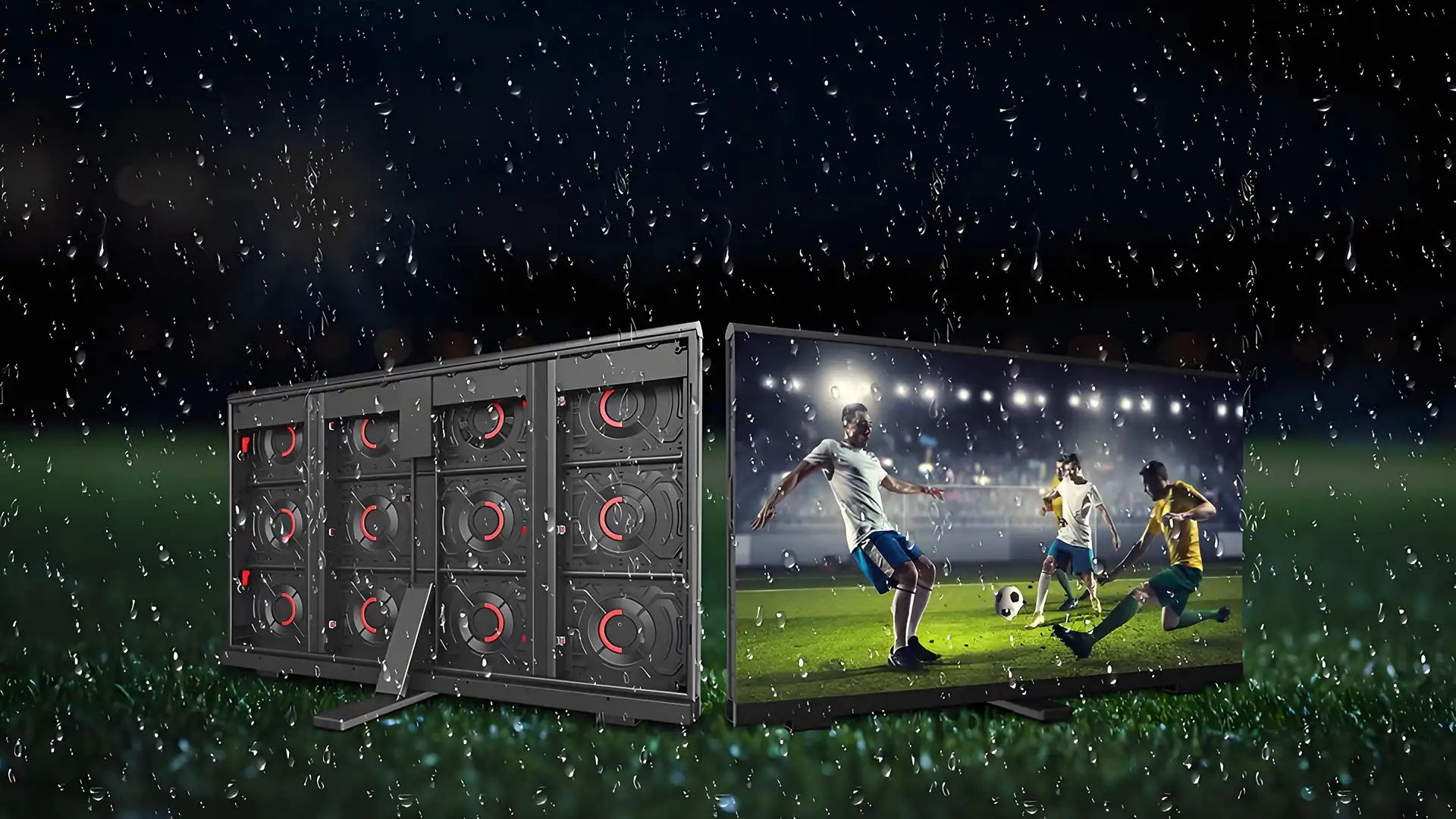
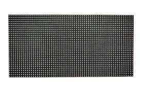
1. Direct View LED Displays: Each pixel comprises individual LEDs. These displays are prevalent in large outdoor billboards, stadium screens, and high-end indoor signage.
2. Micro LED Displays: Utilizing microscopic LEDs as pixels, micro LED technology provides excellent contrast ratio, wide color gamut, and energy efficiency. This emerging technology is promising for next-generation TVs and wearable devices.
3. Mini LED Displays: Mini LEDs serve as backlighting units for LCD panels, offering higher brightness, improved contrast via local dimming, and greater control than conventional LED backlights.
4. OLED (Organic LED) Displays: Although not strictly LED in the inorganic sense, OLED displays utilize electroluminescent organic compounds for each pixel. They provide exceptional color accuracy and viewing angles but require different manufacturing processes.
Core Manufacturing Processes
The production of LED displays involves multiple complex steps that integrate semiconductor fabrication, assembly, testing, and calibration. Key manufacturing stages include:
- Wafer Fabrication: Using semiconductor epitaxy techniques like Metal-Organic Chemical Vapor Deposition (MOCVD), LED chips are grown on substrates such as sapphire or silicon carbide. Parameters like doping concentrations, quantum well layer thickness (typically a few nanometers), and epitaxial layer uniformity directly influence chip efficiency and color output.
- Chip Dicing: Post fabrication, wafers are precisely diced into individual LED dies using laser or mechanical saws. Maintaining minimal kerf width (<30 µm) is essential for yield optimization.
- Die Bonding and Wire Bonding: Each LED chip is mounted on a carrier substrate or PCB using conductive adhesives or solder. Ultrasonic or thermocompression bonding techniques create electrical interconnections. Achieving consistent bond strength and low contact resistance (<30 mΩ) ensures device reliability.
- Encapsulation & Phosphor Application: To protect LED chips and convert light wavelengths (e.g., blue to white), phosphor layers and encapsulants like silicone resins are applied. Uniform phosphor thickness (~10-20 µm) and high optical transparency improve lumen maintenance and color rendering (CRI ≥ 80).
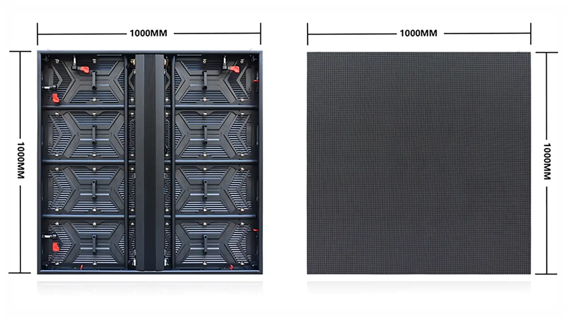
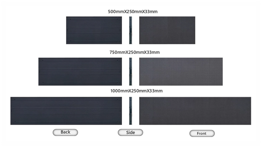
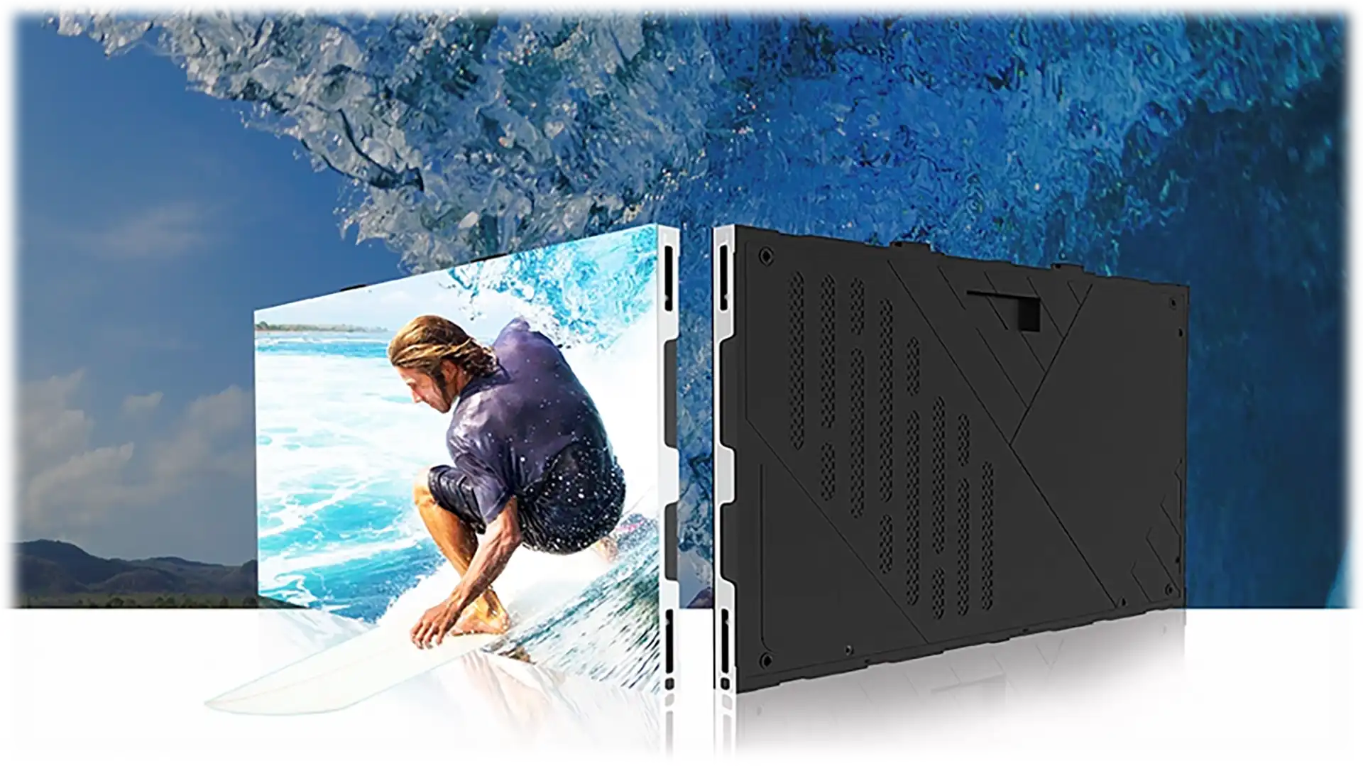
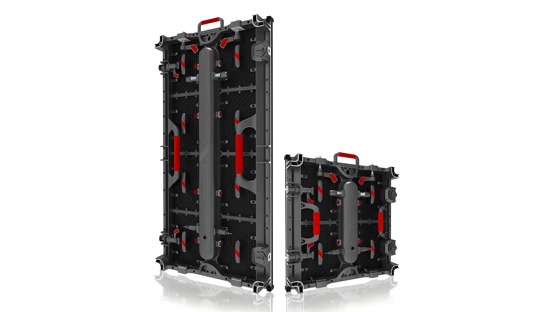
- Module Assembly: LED dies or arrays are integrated into modules with driver ICs, power supplies, and mechanical frames. High Precision Surface Mount Technology (SMT) lines enable placement with ±50 µm accuracy.
- Calibration and Testing: Calibrating brightness, chromaticity coordinates (CIE 1931 x,y), and uniformity is critical. Automated optical inspection systems utilizing CCD cameras and spectroradiometers verify color consistency within DeltaE< 2 across modules.
Technological Innovations Driving Quality
Recent breakthroughs in LED display production enhance performance and reduce costs:
- High-Resolution Pixel Pitch: Contemporary indoor displays achieve pixel pitches as tight as 0.6 mm, allowing retina-quality viewing distances below 1m. Achieving this requires advancements in chip miniaturization, wafer grinding (thinning wafers below 100 µm), and precise alignment.
- Advanced Driver ICs: Integration of multi-channel driver ICs with features like PWM dimming, grayscale control up to 16-bit, and temperature compensation enable smoother gradients and energy savings.
- Thermal Management: Effective heat dissipation is crucial. Manufacturers employ aluminum PCBs, heat pipes, and thermally conductive gels maintaining junction temperature (Tj) below 85°C to prolong LED lifespan (rated up to 100,000 hours).
- Smart LED Displays: Incorporating IoT connectivity and AI-powered calibration dynamically adjusts brightness based on ambient light sensors, reducing power consumption and enhancing viewer comfort.
Compliance with Industry Standards
Adherence to recognized standards ensures product reliability and interoperability. Key standards include:
- IEC 62817: Specifies environmental and mechanical test requirements for LED modules including temperature cycling (-40°C to +85°C), humidity exposure (85% RH), and vibration resistance.
- ANSI/IES LM-79 and LM-80: Define measurement procedures for LED luminous flux and lumen maintenance, respectively.
- RoHS and REACH Compliance: Ensures the use of environmentally safe materials with restricted hazardous substances.
- UL and CE Certifications: Confirm electrical safety and electromagnetic compatibility (EMC).
Case Study: Manufacturing a 2K Indoor LED Display
A recent project involved producing a 2K (1920x1080 pixels) indoor display with a 1.2 mm pixel pitch. Key parameters and process highlights:
- LED Chip Size: 0.2 mm x 0.2 mm
- Brightness: 600 nits calibrated for indoor environments
- Color Accuracy: DeltaE< 2 across full panel
- Process: Utilized wafer thinning to 80 µm, automated die bonding with a cycle time of 3 seconds per die, phosphor coating with uniformity ±3%, and optical calibration using multi-point spectroradiometry.
- Thermal Design: Employed aluminum alloy frame with integrated heat pipes, maintaining cabinet temperature at 45°C under full brightness.
Post-production QA found a module failure rate below 0.1%, surpassing industry benchmarks, demonstrating process control and quality assurance excellence.
Future Outlook
The LED display sector is moving towards:
- Micro LED mass production: Despite current manufacturing challenges, the scalability of micro LED will unlock vibrant, power-efficient displays at consumer scale.
- Flexible and transparent displays: Advanced substrates and bending techniques enable new form factors for automotive and architectural applications.
- Sustainability: Incorporating recyclable materials and energy-efficient processes to reduce carbon footprint.
Conclusion
Sophisticated manufacturing technologies combined with rigorous quality assurance shape the success of the LED display industry. Understanding the interplay between semiconductor physics, process engineering, and system integration is indispensable for engineers aiming to design and produce superior LED display products. Continuous innovation and adherence to international standards pave the way for the next generation of visually stunning, highly reliable LED display solutions.