Advanced Technologies and Manufacturing Processes in LED Display Production
The LED display industry has undergone tremendous evolution over the past decades, driven by rapid technological advancements and growing market demand for high-quality visual solutions across varied applications. As a professional LED display engineer, I will provide a comprehensive analysis of the critical aspects of LED display manufacturing, covering materials, design principles, production processes, and performance parameters. This article aims to offer an authoritative reference for international readers seeking detailed insights into LED display fabrication, emphasizing practical engineering considerations and adherence to industry standards.
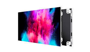
LED (Light Emitting Diode) displays have become indispensable in advertising, event staging, transportation, and control room monitoring due to their superior brightness, energy efficiency, and scalability compared to traditional display technologies. However, manufacturing LED displays involves complex multidisciplinary expertise spanning semiconductor physics, optics, electronics, and materials science.
Key Components and Materials
1. LED Chips: The core of any LED display is the LED chip itself, typically fabricated using III-V compound semiconductors such as Gallium Nitride (GaN) for blue and green LEDs, and Gallium Arsenide (GaAs) for red LEDs. The choice of substrate (sapphire or silicon carbide) impacts cost and performance. Advances in epitaxial growth techniques like Metal-Organic Chemical Vapor Deposition (MOCVD) ensure high crystal quality and uniformity, addressing efficiency droop and thermal challenges.
2. Phosphor Conversion: To achieve white or specialized colors, phosphor coatings are applied for wavelength conversion. Selecting phosphors with high quantum efficiency and thermal stability is crucial. Emerging quantum dot materials offer tunable emission spectra, improving color gamut and luminous efficacy.
3. Encapsulation Materials: The encapsulant protects LED chips from moisture, mechanical damage, and UV degradation. Silicone-based encapsulants with high transparency and thermal stability are preferred, as specified in JEDEC JEP151 for reliability testing.
4. Printed Circuit Boards (PCBs): High-frequency flexible or rigid PCBs with excellent thermal conductivity and controlled impedance are used to mount LEDs and driver circuits, often utilizing materials like Aluminum or Copper MCPCB (Metal Core PCB) to dissipate heat effectively.
Manufacturing Processes
The production of LED displays encompasses several integrated stages, optimized for precision and yield:
- Wafer Fabrication and Testing: Epitaxial wafers undergo photolithography, etching, metallization, and passivation to produce individual LED chips. Wafer-level testing based on parameters like forward voltage (VF), luminous intensity (Iv), chromaticity coordinates (CIE x,y), and electrostatic discharge (ESD) robustness ensures chip quality.
- Chip Sorting and Binning: Chips are categorized into bins according to luminance, wavelength, and forward voltage to enable uniformity in the display panel. This step is critical to minimizing color shifts and brightness inconsistencies.
- Assembly and Packaging: Individual LEDs are mounted onto PCB substrates using automated pick-and-place machinery. Wire bonding or flip-chip packaging methods connect electrical contacts, followed by encapsulation and curing. Industry standards such as JEDEC J-STD-020 govern moisture sensitivity to prevent failure.
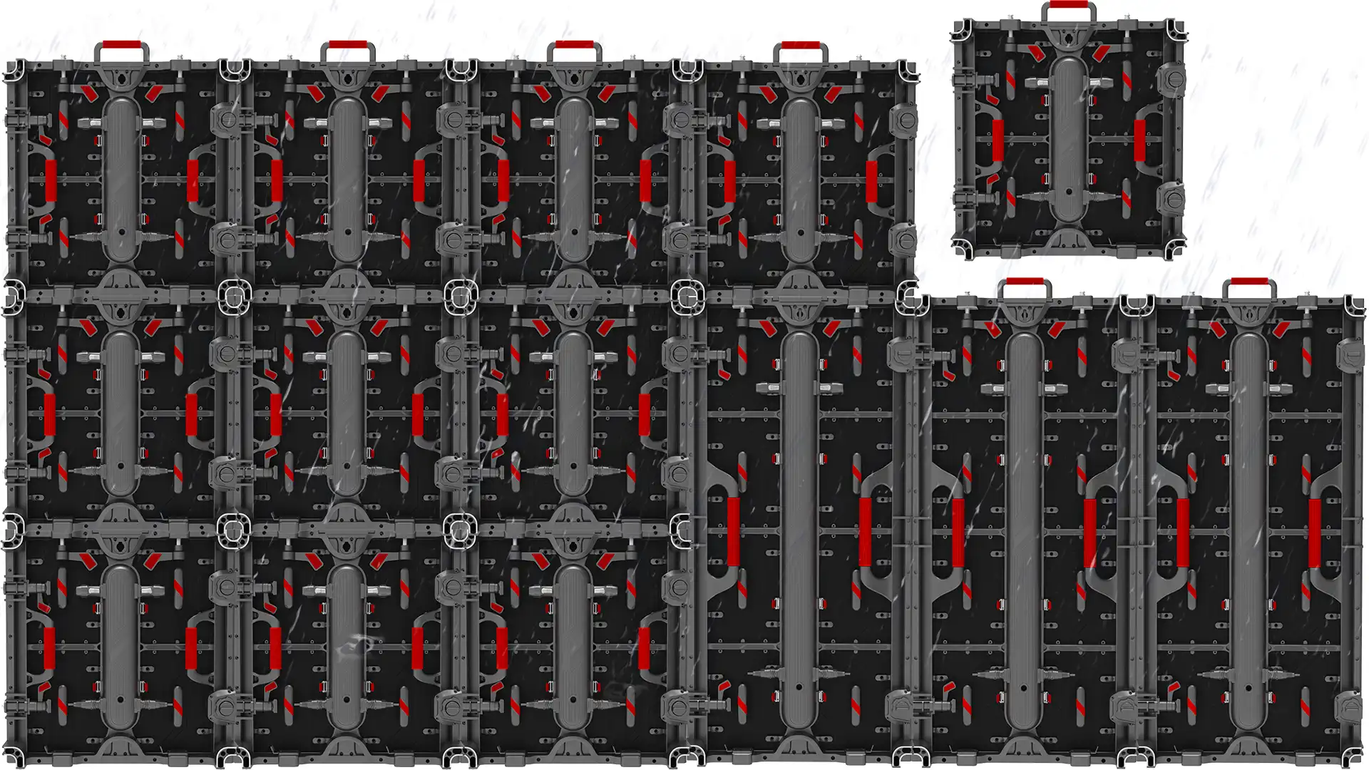
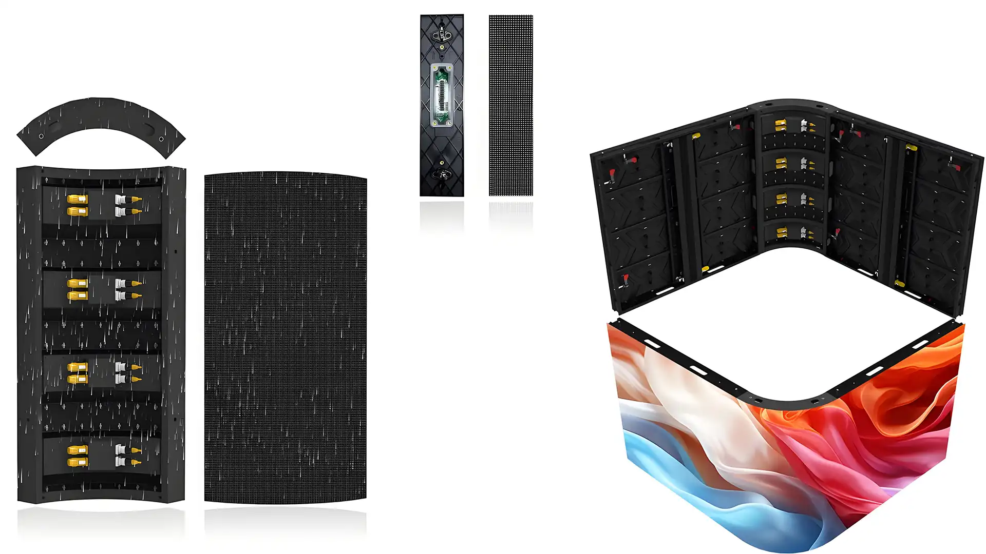
- Module Integration: LED modules combining multiple LED arrays with driving ICs, optical lenses, and power management units are constructed to form display panels. Precision soldering, component placement, and cleaning are essential to maintain signal integrity and thermal management.
- Calibration and Testing: Post-assembly calibration using spectrometric equipment and automated image analysis ensures consistent color temperature, brightness, and gamma correction. Environmental stress tests (thermal cycling, humidity exposure) following IEC 62087 validate operational reliability.
Technical Parameters and Performance Metrics
An engineered LED display's quality is defined by several parameters:
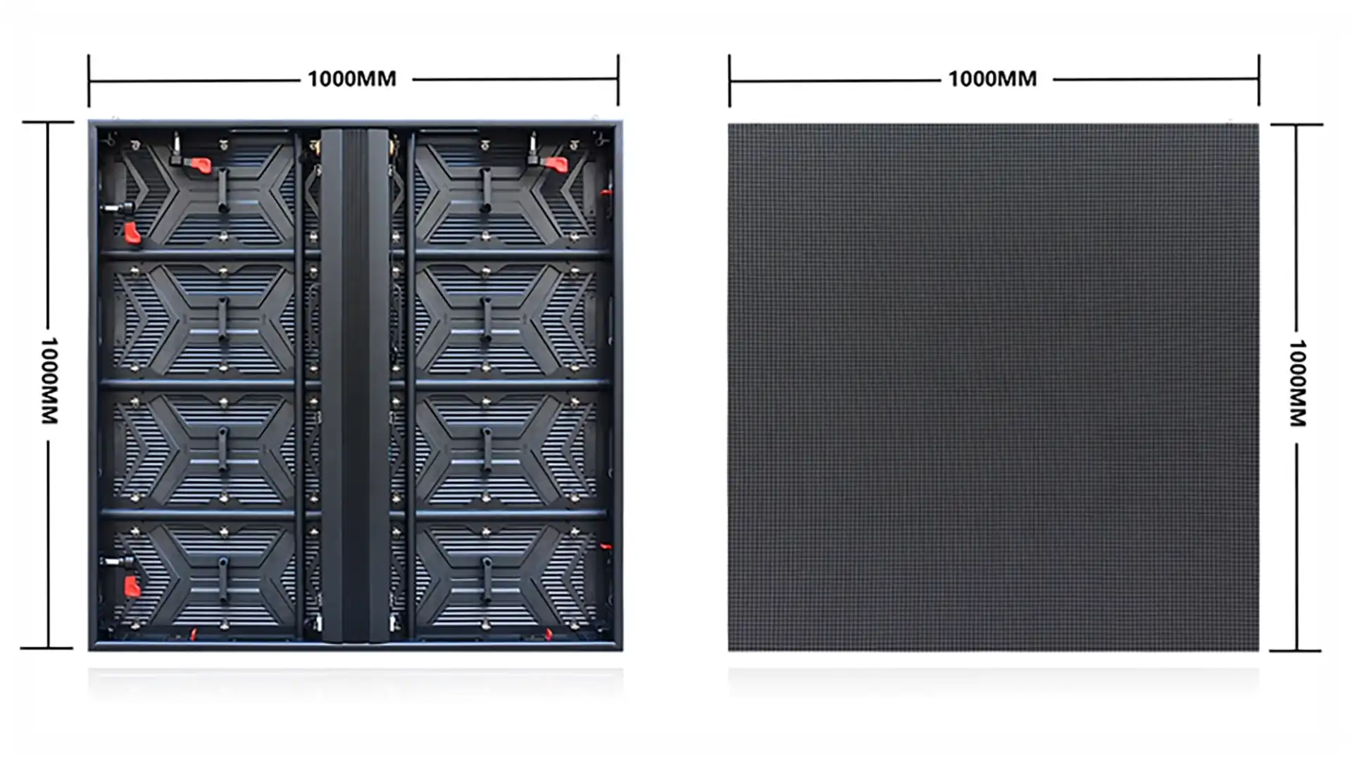
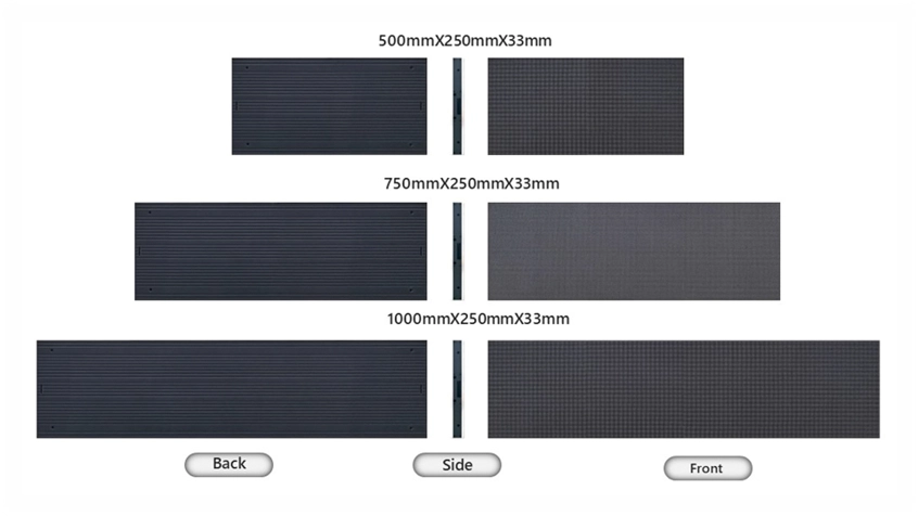
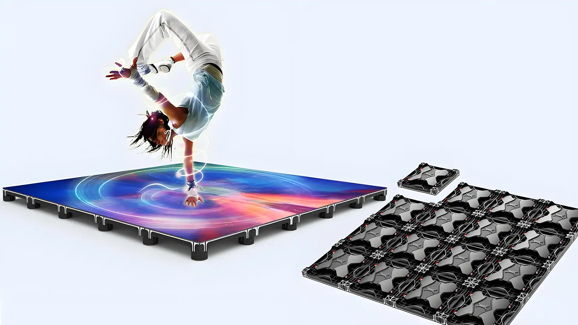
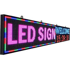
- Pixel Pitch: The center-to-center distance between adjacent pixels, critical for resolution and viewing distance. Typical ranges include P0.9mm (fine pitch) to P20mm+ (outdoor signage).
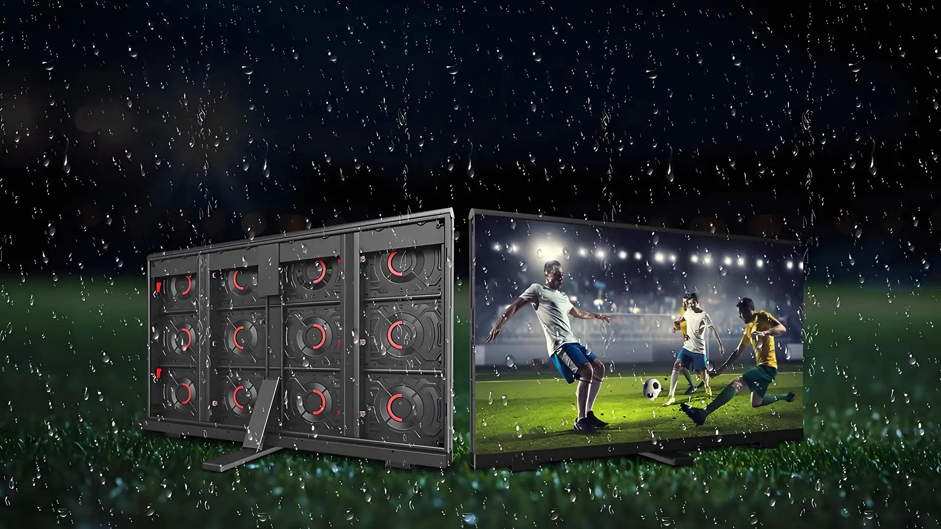
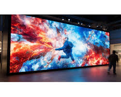
- Brightness: Measured in nits (cd/m²), outdoor displays require luminance above 5000 nits to overcome ambient light, while indoor displays typically range between 800 to 1200 nits.
- Refresh Rate: High refresh rates (>1920 Hz) enable flicker-free video and are essential for broadcast and high-speed imaging applications.
- Color Gamut: Percentage coverage of color spaces (sRGB, AdobeRGB) determines image vibrancy and fidelity. Advanced displays achieve 95%+ NTSC coverage using quantum dot or phosphor technology.
- Power Consumption: Efficient driver circuitry and LED chip design minimize electrical usage, with power densities typically between 300-600 W/m².
- Viewing Angle: Wide horizontal and vertical angles (>160°) ensure consistent brightness and color from different perspectives.
Emerging Trends and Innovations
Several cutting-edge developments are shaping the future of LED display manufacturing:
- MicroLED Technology: Offering pixel-level inorganic LEDs with superior brightness, contrast, and longevity. Manufacturing challenges include microscopic chip handling and mass transfer.
- Flexible and Transparent Displays: Utilizing flexible PCBs and OLED hybrid technology for curved or see-through applications in automotive and architecture sectors.
- AI-Driven Manufacturing: Integration of artificial intelligence for defect detection, process optimization, and real-time quality control enhances yield and reduces costs.
- Sustainability Initiatives: Emphasizing recyclable materials, reduced chemical usage, and energy-efficient manufacturing lines align with global environmental standards such as RoHS and WEEE directives.
Case Study: High-Resolution Indoor LED Display Manufacturing
A leading manufacturer producing a P1.2mm indoor LED display module optimized the binning process by implementing dynamic spectral sorting using in-line spectrometers. This innovation reduced color variation by 35%, enhanced panel-wide uniformity, and shortened calibration times by 20%, resulting in improved customer satisfaction and decreased manufacturing costs.
Industry Standards and Compliance
Adhering to international standards ensures reliability and interoperability:
- IEC 62031: LED modules for general lighting – safety requirements.
- JEDEC JEP51 & JEP151: Measures for LED chip lifetime and moisture sensitivity classification.
- CIE 1931 Color Space: Standardized system for color measurement.
- ISO 9001: Quality management systems certification for manufacturing consistency.
In conclusion, manufacturing advanced LED displays involves a meticulous integration of semiconductor fabrication, optical engineering, precision assembly, and rigorous quality control governed by international standards. Continuous innovations in materials and processes drive LED displays towards higher performance, sustainability, and diverse application possibilities. Practitioners in this field must emphasize holistic design principles and robust manufacturing protocols to meet the evolving demands of the global market.