Advanced Technologies and Best Practices in LED LCD Screen Manufacturing
The LED LCD screen industry has experienced remarkable advancements over the last decade, driven by evolving display technologies and increasing demand for high-quality visual experiences across various sectors, including consumer electronics, digital signage, automotive displays, and industrial interfaces. As an LED display engineer with extensive experience, the objective of this article is to delve into the critical technical parameters, manufacturing processes, and industry best practices that define modern LED LCD screen production, ensuring optimal performance, reliability, and user satisfaction.
Introduction
The fundamental architecture of an LED LCD (Light Emitting Diode Liquid Crystal Display) screen merges two key technologies: the LCD panel providing image modulation based on liquid crystal cells, and the LED backlighting that illuminates the display. This synergy achieves superior brightness, color gamut, energy efficiency, and lifespan compared to older CCFL (Cold Cathode Fluorescent Lamp) backlighting methods. Understanding the latest innovations in LED LCD manufacturing is essential for engineers and manufacturers aiming to produce displays that meet rigorous quality and performance standards set by industry bodies like the International Electrotechnical Commission (IEC) and Society for Information Display (SID).
Main Body
1. Technical Parameters and Material Selection
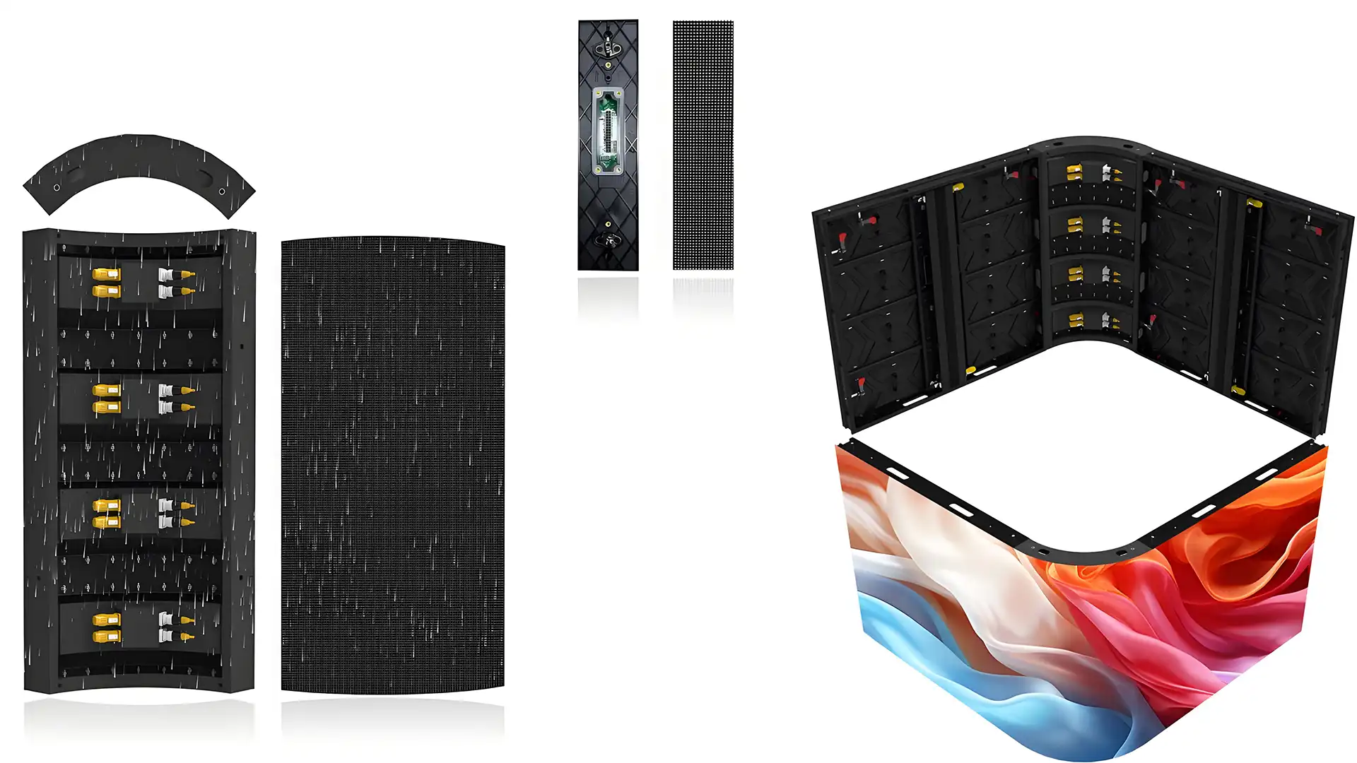
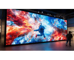
One of the foremost considerations in LED LCD manufacturing is the selection of appropriate LED backlight units (BLUs). Typically, BLUs consist of surface-mount device (SMD) LEDs arranged to provide uniform brightness and color temperature across the screen. Commonly, display brightness ranges from 300 to 1000 cd/m² for indoor applications, and up to 2500 cd/m² or more for outdoor or automotive displays. High CRI (Color Rendering Index) LEDs with a color temperature between 5500K and 6500K are preferred to produce vivid, natural colors.
The LCD panel itself utilizes thin-film transistor (TFT) technology, primarily amorphous silicon (a-Si) or low-temperature polysilicon (LTPS), each offering distinct advantages. LTPS TFTs provide higher electron mobility for faster refresh rates and better pixel response times, indispensable for high-resolution displays exceeding 4K UHD standards.
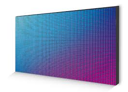
Another crucial parameter is the native contrast ratio, which depends on the liquid crystal alignment and polarizer quality. Modern IPS (In-Plane Switching) panels achieve contrast ratios around 1000:1, with some VA (Vertical Alignment) panels offering even higher contrast, suitable for HDR (High Dynamic Range) content. The integration of local dimming technology, where LED backlight zones independently vary their brightness, further enhances contrast and reduces halo effects.
2. Manufacturing Processes and Quality Control
Precision in assembly is vital to mitigate issues such as mura (uneven brightness) and color shifts. The manufacturing sequence includes layer stacking — polarizers, glass substrates, liquid crystals, and LED backlight units — along with bonding and sealing under controlled cleanroom conditions to prevent contamination.
Advanced manufacturing lines utilize inline inspections with charge-coupled device (CCD) cameras to detect pixel defects (e.g., stuck or dead pixels), uniformity inconsistencies, and alignment errors. Industry standards such as ISO 9241-307 specify pixel defect classification, critical for product grading and customer acceptance. Furthermore, adherence to RoHS (Restriction of Hazardous Substances) and REACH (Registration, Evaluation, Authorization, and Restriction of Chemicals) directives ensures environmental compliance, enhancing product marketability.
Post-assembly testing includes thermal cycling and humidity testing according to IEC 60068 standards to verify durability under extreme conditions. Additionally, specialized Electromagnetic Interference (EMI) shielding and reliability testing guarantee the display's functionality without disturbing nearby electronic devices.
3. Innovations and Emerging Trends
Mini-LED and Micro-LED technologies have revolutionized LED LCD displays by enabling thousands of individually controllable local dimming zones, drastically improving contrast ratios often exceeding 50000:1. These advances are critical for applications such as medical imaging and professional content creation that demand unparalleled color accuracy and brightness.
Moreover, quantum dot enhancement films (QDEF) have become mainstream within LED LCD manufacturing, significantly expanding the color gamut beyond standard Rec. 709 to the wider DCI-P3 or even Rec. 2020 standards. This development affords displays the ability to render ultra-realistic imagery while maintaining energy efficiency.
Manufacturers are also leveraging AI-driven process controls and predictive maintenance algorithms, ensuring yield maximization and material waste reduction. This aligns well with Industry 4.0 initiatives, fostering smarter factories capable of real-time quality monitoring and adaptive manufacturing workflows.
Conclusion
In conclusion, the manufacture of LED LCD screens today demands a holistic integration of material science, precision engineering, and rigorous quality assurance processes to meet global market expectations for performance and reliability. Advances in LED technologies such as Mini-LED and quantum dots continue to push the boundaries of display capabilities, setting new benchmarks for brightness, contrast, and color fidelity.
Successful LED LCD manufacturing is underpinned by adherence to international standards, sophisticated production equipment, and continuous R&D investment. The future trajectory points towards flexible and transparent LED LCD panels optimized for next-generation applications, including smart wearables, automotive HUDs (Head-Up Displays), and AR/VR systems. For engineers and manufacturers, staying abreast of these trends and embedding best practices will be essential to maintain competitive advantage in this dynamic industry.