LED Display Technology: Advanced Engineering, Manufacturing, and Industry Insights
In the rapidly evolving world of digital displays, LED (Light Emitting Diode) technology stands at the forefront of innovation, providing unmatched brightness, energy efficiency, and lifespan compared to conventional display systems. As an experienced LED display engineer, this article delivers an in-depth exploration of LED display manufacturing processes, technical parameters, and recent industry advances, drawing upon authoritative standards and real-world case studies for international applications.
Introduction
The global LED display market has witnessed exponential growth driven by diverse applications ranging from advertising billboards and sports arenas to indoor dynamic signage and consumer electronics. According to the International Electrotechnical Commission (IEC) standards and the American National Standards Institute (ANSI), LED displays must not only meet luminous intensity and color accuracy requirements but also adhere to stringent durability and energy consumption criteria. Understanding fundamental LED screen manufacturing principles and engineering practices is crucial to maintaining quality and performance across varied use cases.
Core Components and Design Principles
LED displays consist primarily of individual LED pixels arranged in a matrix, controlled via dedicated driver ICs. Each pixel combines red, green, and blue diodes with specific luminous intensities—measured in nits (cd/m²)—to generate full-color images through additive color mixing. Typical high-performance LED displays achieve brightness levels of 1000 to 5000 nits, ensuring visibility across indoor and outdoor environments.
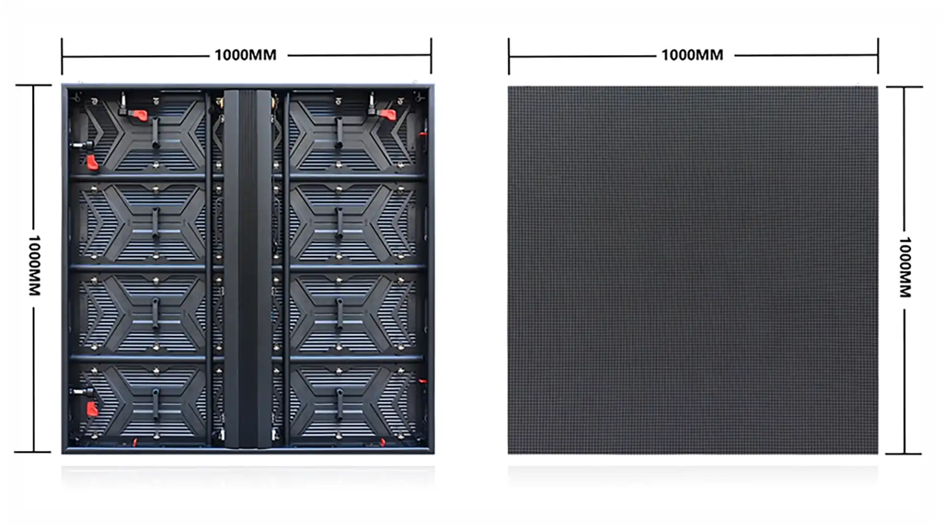
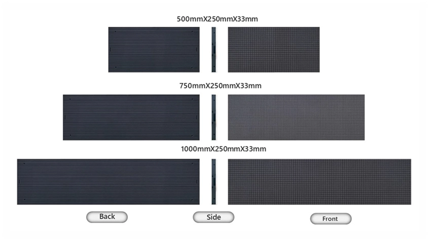
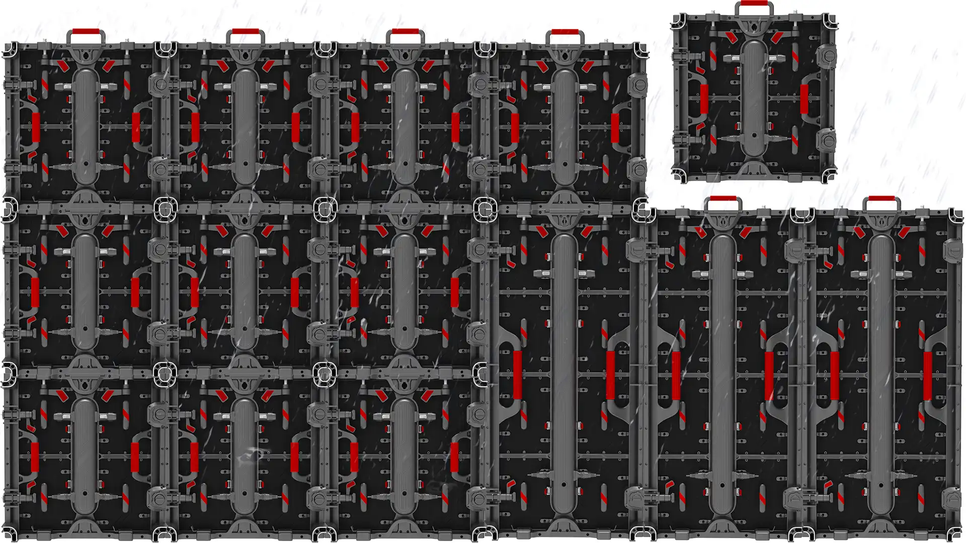
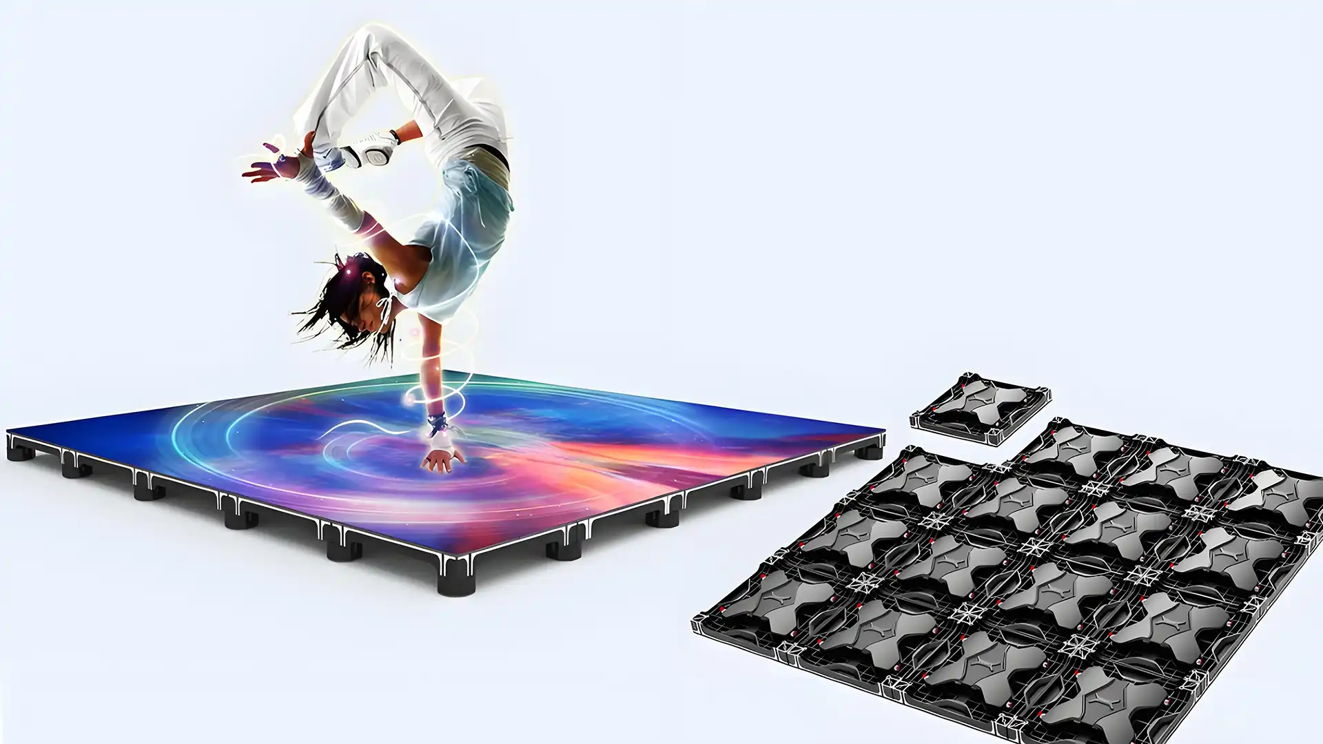
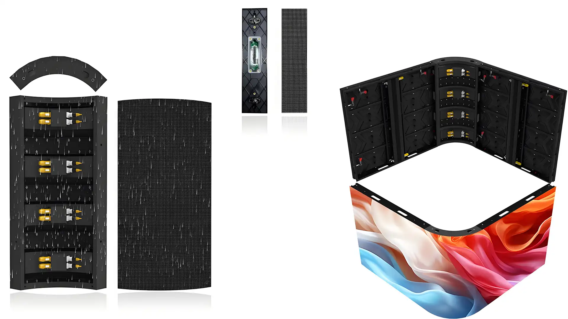
Industrial-grade designs incorporate high-PPI (pixels per inch) density ranging from 60 to 3840 PPI to accommodate applications from large-format billboards to ultra-fine pixel displays for broadcast and close-viewing purposes. Pixel pitch—the distance between the centers of adjacent pixels—plays a significant role in image clarity and typically ranges from 0.9mm (for indoor LED LCDs) to 25mm (outdoor LED displays).
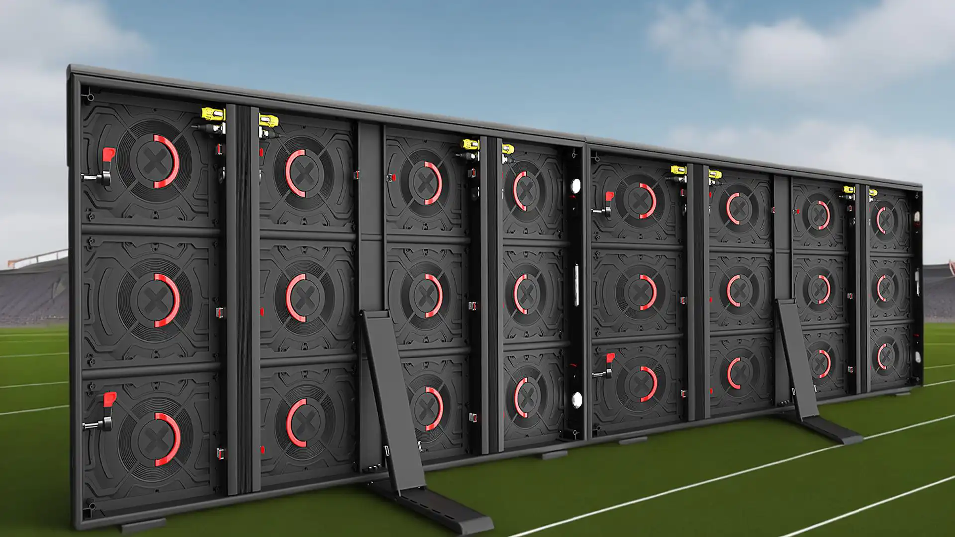
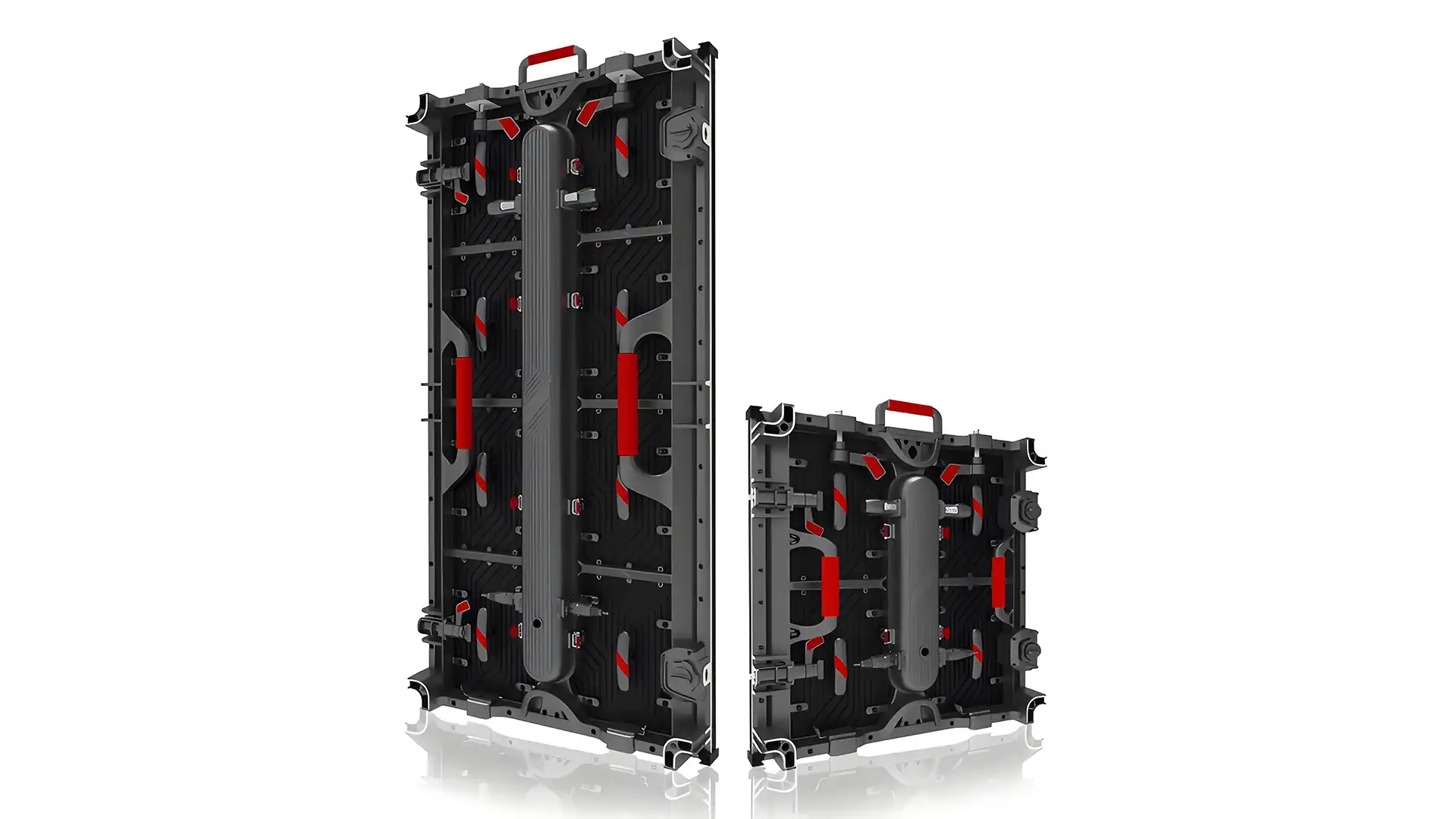
Manufacturing Process and Quality Control
The precision manufacturing of LED displays involves several critical steps:
1. LED Chip Fabrication: Semiconductor wafers using materials such as Gallium Nitride (GaN) or Indium Gallium Nitride (InGaN) are grown using Metal-Organic Chemical Vapor Deposition (MOCVD), followed by dicing into individual LED chips.
2. Module Assembly: LEDs are mounted on Printed Circuit Boards (PCBs) with rigorous attention to electrical connectivity and thermal dissipation. Automated pick-and-place machines handle the accurate placement of thousands of LEDs per module.
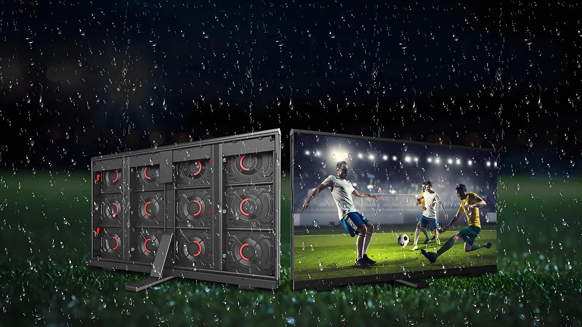
3. Encapsulation and Coating: To enhance weather resistance and longevity—often rated from IP54 to IP67 for outdoor products—LED modules undergo advanced encapsulation techniques involving silicone potting and UV-resistant coatings.
4. Calibration and Testing: Calibration systems correct color and brightness uniformity per pixel. Industry norms, such as the Digital Display Measurement Standards (DDMS), require luminance and chromaticity testing to ensure conformance. Thermal testing ensures stability over extended operation.
Technical Parameters and Performance Metrics
LED display specifications often include:
- Brightness: 1000–10000 nits (outdoor models at upper scale)
- Contrast Ratio: Above 1000:1, critical for vivid imaging
- Refresh Rate: ≥ 1920 Hz to eliminate flicker in broadcast-grade displays
- Viewing Angle: Typically 140° horizontal and vertical for uniform clarity
- Power Consumption: Between 350 to 700 watts per square meter, optimized for energy-efficient designs
- Lifetime: Rated 100,000 hours minimum under standard operating conditions
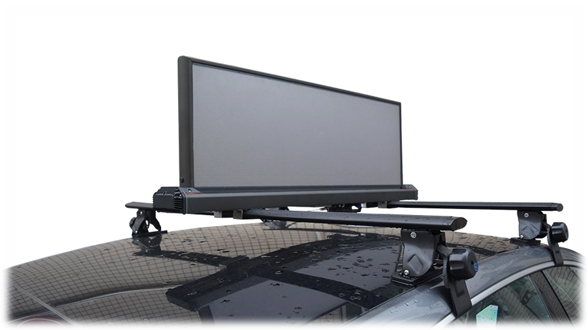
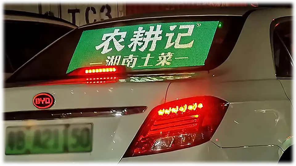
Case Study: Large-Scale Outdoor LED Display
A recent project involved deploying a 500-square meter LED display at an international sports stadium. The screen utilized 10mm pixel pitch SMD (Surface-Mounted Device) modules with IP65-rated waterproofing. Integrated automatic brightness adjustment sensors ensured optimal visibility under varying sunlight intensities. Through strict compliance with IEC 62087 (methods of measurement for power consumption) and IEC 62717 (performance standard for LED modules), the installation achieved 80% energy savings compared to traditional floodlighting solutions.
Future Trends and Innovations
Emerging trends include MicroLED technology offering ultra-fine pixel densities below 0.5mm pitch, promising unprecedented image sharpness and durability. Integration with AI-based calibration systems and advanced thermal management materials are set to further enhance display efficiency and longevity. Industry standards continue to evolve, emphasizing sustainability and recyclability in panel components to meet global environmental targets.
Conclusion
LED display engineering combines sophisticated semiconductor manufacturing techniques, precision assembly, rigorous testing, and adherence to international standards to produce reliable and high-performance visual solutions. Whether for indoor retail advertising or massive outdoor installations, understanding technical parameters and maintaining quality controls are essential for advancing the industry. With ongoing innovations and system-level integrations, LED displays remain pivotal in the future of dynamic, energy-efficient digital media.