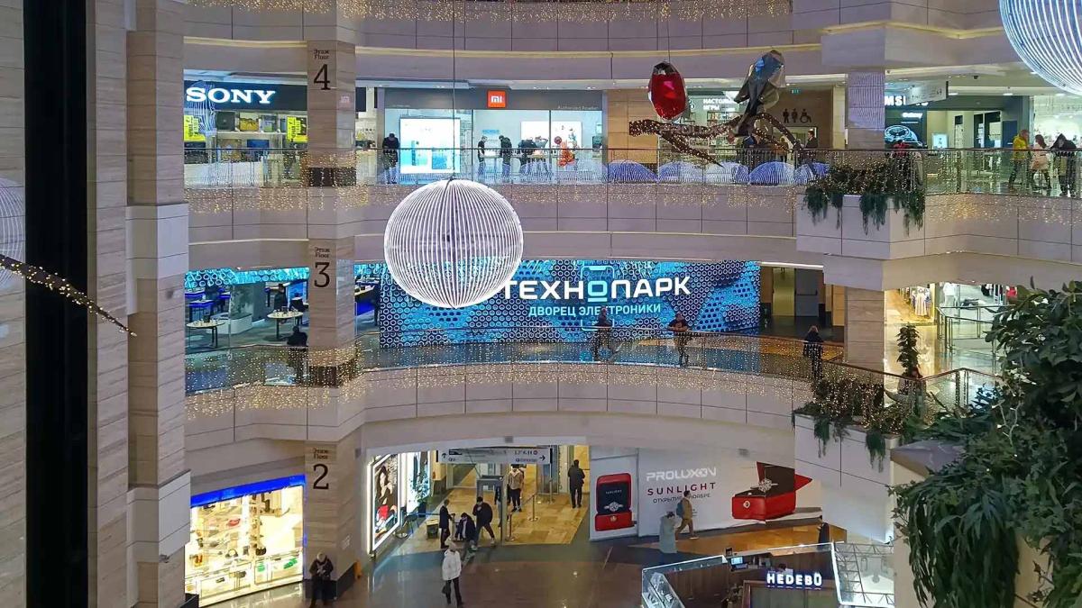
What is the Status of Micro LED Display Progress for Mass Production in 2023?
The year 2023 marks a critical milestone for Micro LED as a display technology, with only two months remaining. After years of dedicated research, development, and refinement, Micro LED technology is poised to achieve technological maturity in 2023. This advancement encompasses enhanced LED chip density, reduced LED size, heightened brightness levels, and improved energy efficiency. These remarkable technological enhancements empower Micro LED to excel in large-scale displays while effectively meeting market demands.
Over the past few years, Micro LED display technology has undergone a significant transition from laboratory research to commercial products. Numerous companies have successfully developed prototypes of Micro LED displays and showcased their potential in public demonstrations. This accelerated transformation of research and development outcomes will play a crucial role in further promoting the mass production of Micro LED. What breakthroughs has Micro LED achieved in this pivotal year?
01.The cost of Micro LED is experiencing a continuous decline.
Micro LED, as a new display technology, incorporates the advantages of OLED and LCD while facing challenges in mass production and high cost. According to recent market research, the current cost for 10-14 inch Micro LED panels can range from $6,000 to $10,000 per panel. This equates to approximately RMB 71,800 for a single panel. The high cost has impeded the development of Micro LED; therefore it is imperative that costs decrease in order to expand market potential. Many companies are currently focusing on chip development.
Firstly, Micro LED employs chips smaller than 100 microns in size. In theory, the reduction in chip size leads to a decrease in material costs. It is estimated that over the next four years, Micro LED chips can achieve an annual cost reduction of at least 20% to 25%. Therefore, reducing chip size serves as the primary approach for cost reduction. Secondly, companies are exploring ways to minimize material expenses by enhancing the materials required for Micro LED displays and seeking more economical and sustainable alternatives to reduce raw material costs. Currently, most market applications utilize PCB boards which incur relatively high costs. To address this issue, companies like BOE and Leyard are conducting research on glass substrates as potential replacements for PCB boards with the aim of cost reduction.
02. The advancements in large-scale transfer technology and the intensity of red light have achieved significant breakthroughs.
One of the major challenges associated with Micro LED technology is the issue of yield. Numerous manufacturers are making concerted efforts to address this critical problem. Laser transfer technology, which boasts a significantly higher yield rate compared to traditional stamp transfer technology, holds great promise for overcoming this challenge. Mass transfer technology was previously considered a bottleneck due to its difficulty in achieving a transfer yield of 99.9999% (commonly referred to as "six nines") and ensuring an accuracy within plus or minus 0.5 μm for each chip. However, significant improvements have been made in this area over the past two years. Presently, Micro LED displays can be seamlessly integrated into ultra-large screens for home use; however, further breakthroughs are required when applying them in the field of augmented reality (AR).
Recently, the University of Strathclyde in the UK announced a novel mass transfer technology for Micro LED. Researchers claim that by employing continuous roller transfer technology, they can achieve mass integration of Micro LED with a single transfer. The 320x240 pixel array corresponds to over 75,000 Micro LEDs. The relative position accuracy reaches sub-micron level while preserving the geometric structure of the pixel array. The deviation between pixel spatial positioning error and design layout is controlled within 1 μm.
According to news released on October 8, 2023, Shanghai Jade Bird Display (referred to as "JBD" hereafter), a prominent manufacturer in Micro LED technology, announced that their independently developed 0.13-inch MicroLED red light chip has surpassed the milestone of 1 million nits in brightness, once again setting a new industry record. It is reported that JBD achieved this remarkable achievement by making significant breakthroughs in various technologies including material growth technology, non-radiative composite suppression technology, and beam divergence angle control.
03. The new packaging technology demonstrates excellent performance.
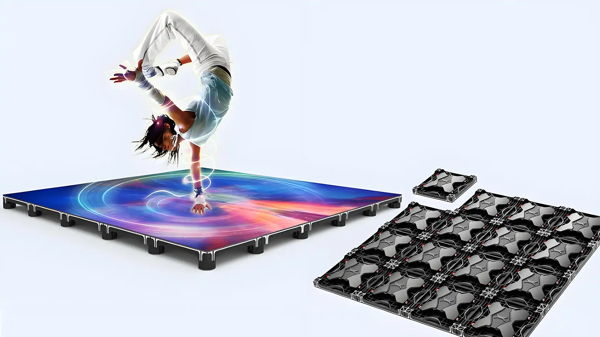
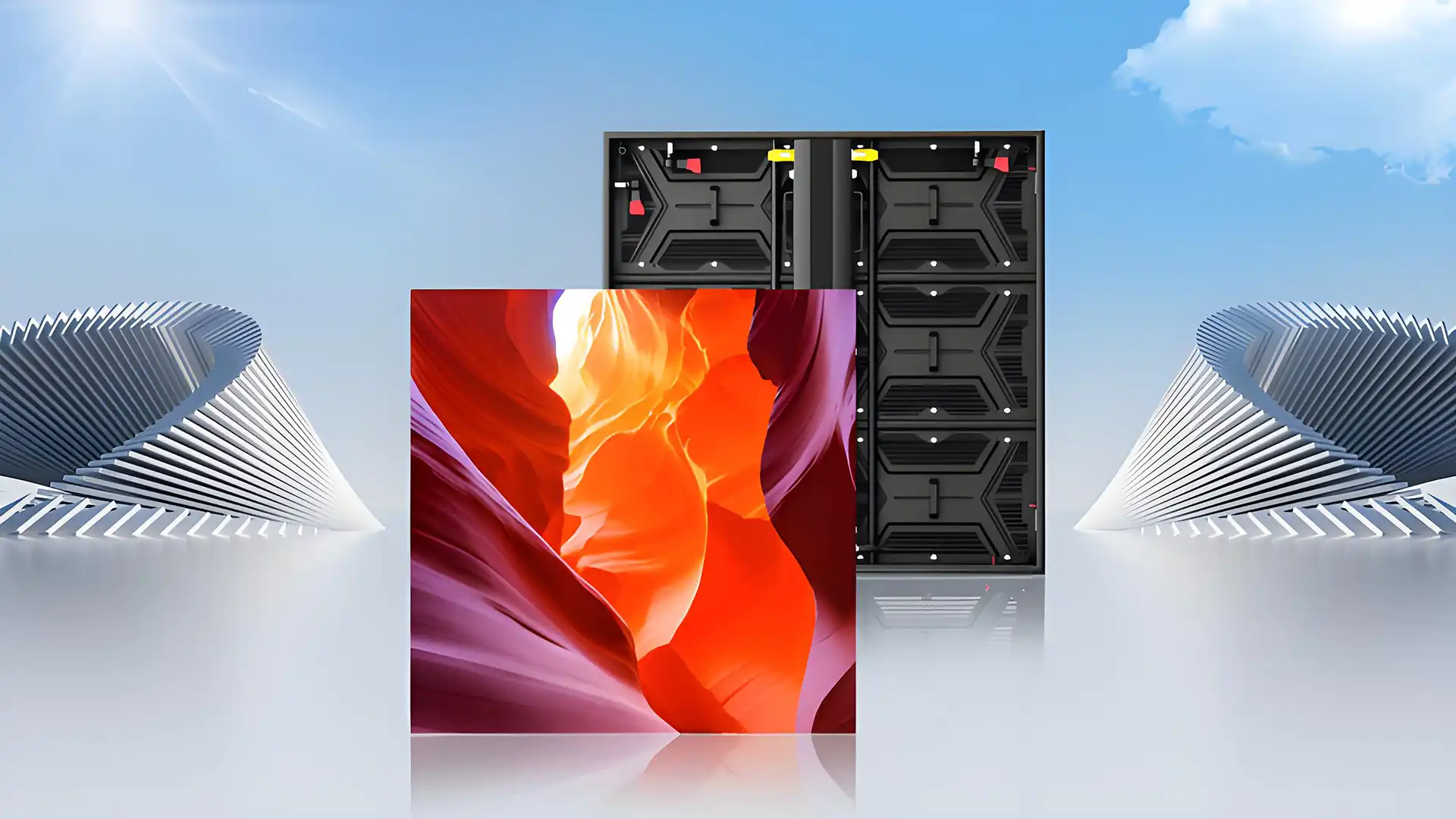
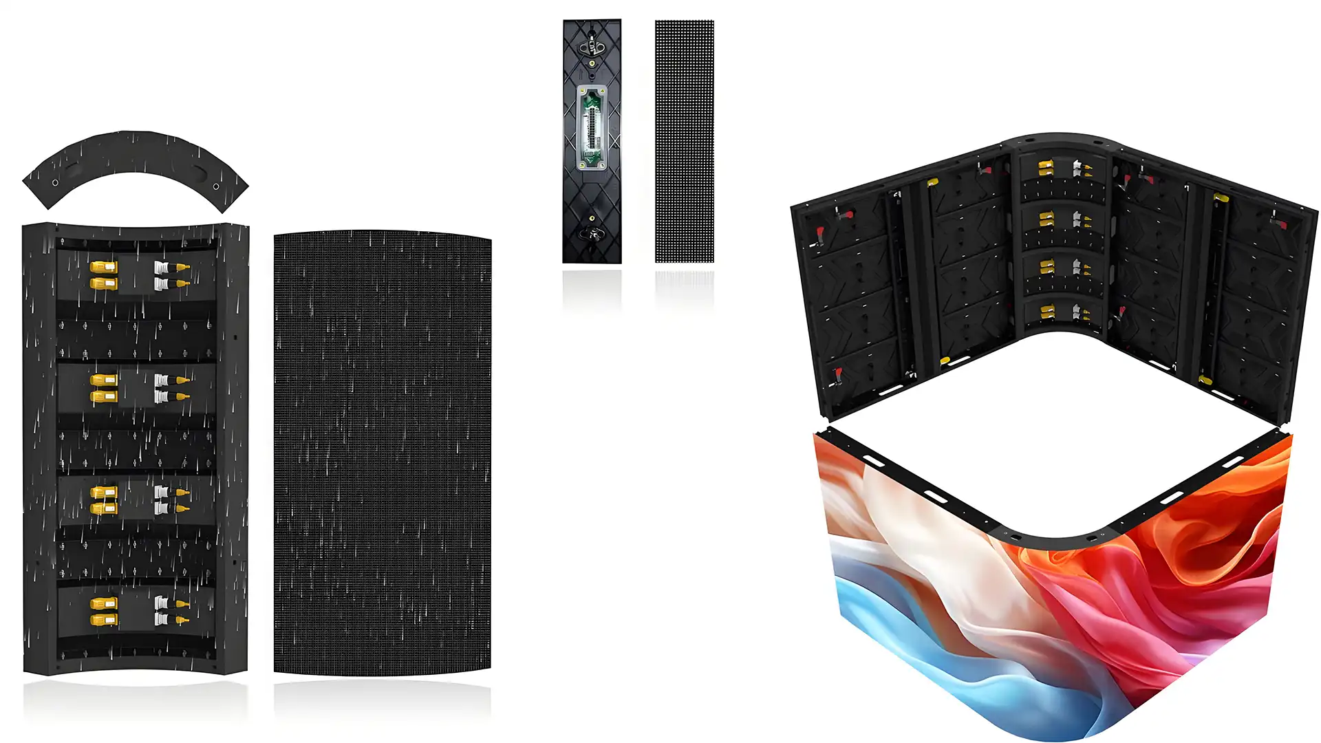
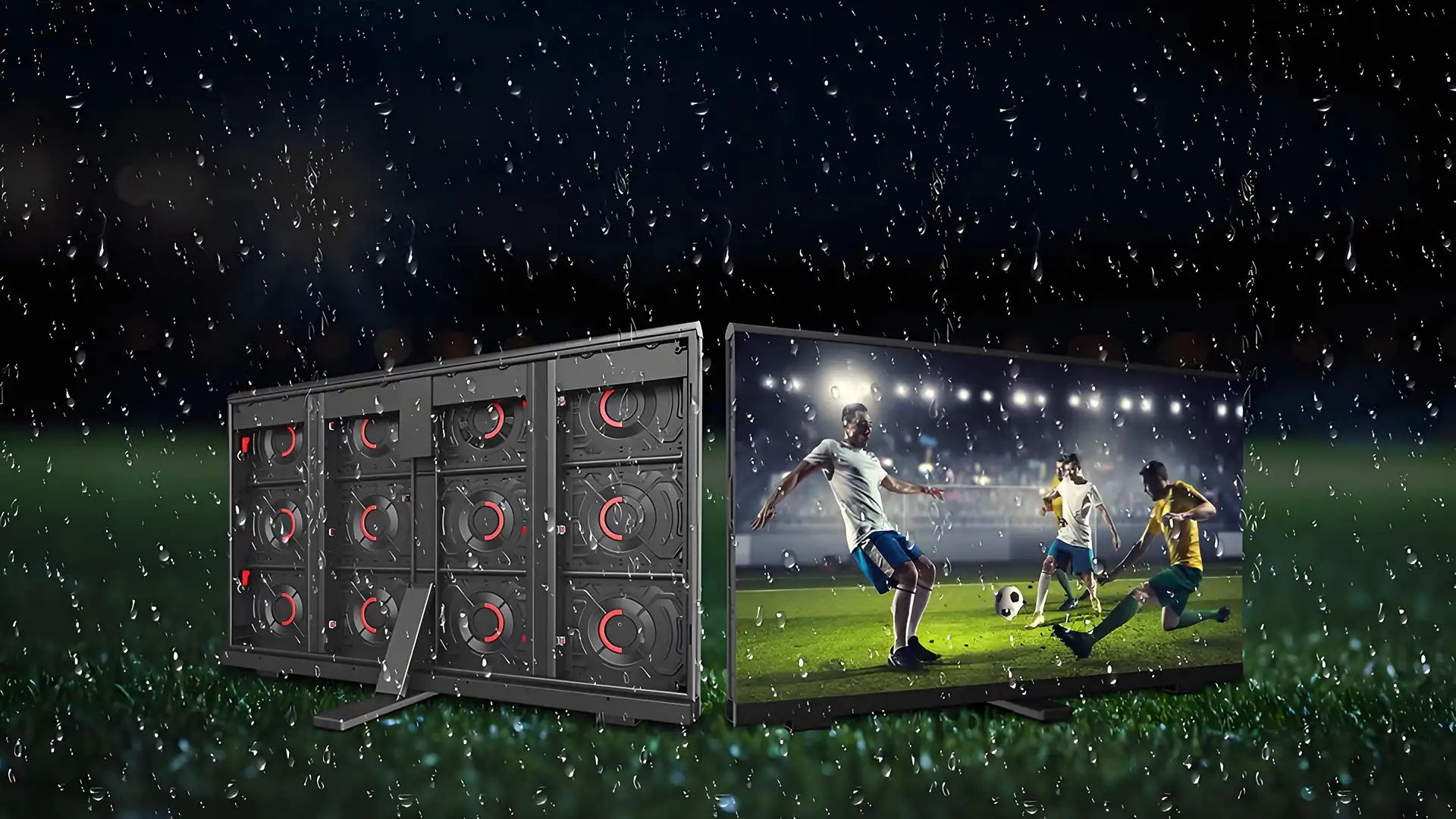
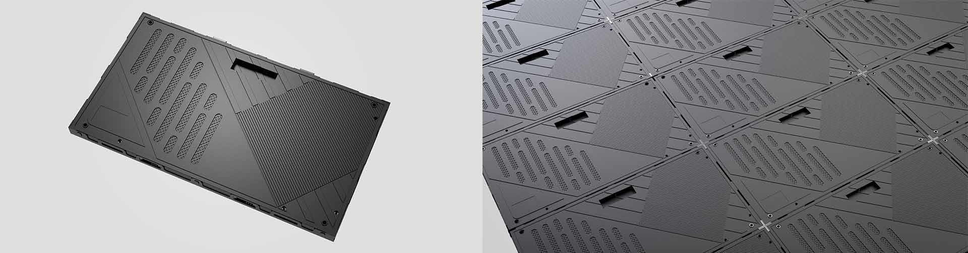
The MIP technology has emerged as an optimal solution for Micro LED applications. MIP, short for Micro LED In Package, represents a cutting-edge packaging technique that involves the transfer of Micro LED chips onto a carrier board through advanced mass transfer technology. The subsequent steps include precise packaging, segmentation into smaller units, and meticulous mixing to achieve uniform illumination. Furthermore, this process seamlessly integrates surface coating capabilities for screen enhancement and facilitates the seamless production of high-quality display screens, weclome to inquiry KSSDISPLAY COB and MIP LED displays.
The MIP technology boasts numerous advantages, including light mixing, high uniformity, and absence of the Mura effect. It eliminates the need for costly repairs, can be directly tested and sorted, and simplifies point testing and sorting. Moreover, it offers unique benefits in terms of compatibility with large-scale mass production of large-size Micro LEDs as well as acceptance by terminal display manufacturers. In scenarios where smaller spacing and larger sizes are required for terminal displays, MIP is an ideal choice that circumvents core bottlenecks related to yield, ink color consistency, uniformity inspection and repair costs.
In terms of LED chip size requirements, SMD and COB packaging is limited to bilateral sizes greater than 100μm, whereas MIP packaging can accommodate LED chips as small as 60um. The mainstream SMD size for lamp beads is generally above 1010 under normal circumstances, whereas the corresponding main size of MIP is currently smaller than 0808. The point spacing of MIP can be minimized at the display level, followed by COB, while SMD is more significantly restricted in terms of point spacing.
Generally speaking, MIP outperforms SMD and COB in terms of LED chip size, electrical connection, contrast, mounting process, repairability, flatness, mixed light bins, etc. It can be observed that MIP is particularly suitable for smaller chips with ample room for reducing spacing and cost. The future trajectory of Micro LED is thus determined with MIP showcasing evident advantages.
It is widely acknowledged in the market that Micro LED technology is currently in its infancy stage for large-scale commercial use, and it may not experience a significant market explosion until after 2025. Although it remains challenging to predict when Micro LED will be commercially viable on a larger scale, the fact that many screen companies have invested in the Micro LED industry chain bodes well for advancing this process and providing optimal solutions. As components continue to improve, manufacturing processes are optimized through better equipment and technological breakthroughs, coupled with mass production and diversified applications; more manufacturers are expected to invest in this field by 2024. While enhancing the supply chain, they will also further optimize the cost structure of Micro LED. Weclome to inquiry KSSDISPLAY COB and MIP LED displays.
Since each generation of technology corresponds to a specific target market, it is unlikely that any particular technology will dominate in the coming years. However, it is certain that Micro LED holds immense potential as the future display technology leader, and manufacturers who proactively adopt related technologies will continue to reap significant benefits.
Links: COB Display | MIP Display | Indoor Display | LED Display Videos